The photodiode is a cheap surface mount silicon unit VBP104S, RS part number 768-9394. From the datasheet what is the active area of the photodiode?
Length: 6.4mm Height 3.9mm
https://www.vishay.com/docs/81170/vbp104sr.pdf
What is the maximum current in D1 and D2?
If we assume our operating voltage is roughly around the max reverse: 60V
Our should be equal to
The photodiode produces an output voltage of 1V peak across RPD. Choose a value for RPD
The maximum analogue input to AIN is 3.3V. Choose values of R2 and R1 so that the required maximum input voltage to AIN is achieved. Note that R2 = R2’ and R1 = R1’
What is the maximum current in G4 and G7?
From the datasheet of the 78M33 (RS part number 809-5472) what is the maximum current in G1?
6mA
A1 and A2 are type MCP6L01T-E/LT RS part number 768-1397. What is the maximum current in G3, G6?
+- 2mA
M1 and M2 draw up to 1A each. What is the maximum current in G10?
2A (1+1A)
The L298 is RS part number 636-384. What is the maximum current in G9? (Hint: It is equal to the maximum quiescent current in VS + the maximum quiescent current in VSS)
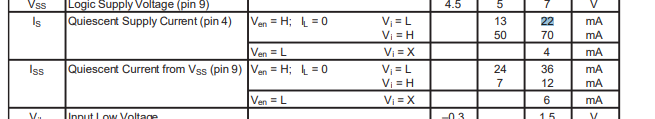 82mA
82mA
What is the maximum current in G0?
G0 = G1 + G2 + G3 + G4 + G5 + G6 + G7 + G8 + G9 + G10
G1 = 6mA G2 = G5 = 3.58mA G3 = G6 = 2mA G4 = G7 = 0.1mA G8 = 20mA (in first page for FRDM board) G9 = 82mA G10 = 2A
G0 = 2.12A
What is the typical resistance of a wire on a typical PCB? (Use this value for all subsequent calculations)
0.123
What voltage corresponds to a change in the least significant bit in the ADC input AIN? Note that the FRDM KL-25Z has a 16 bit ADC
What voltage corresponds to a change in the least significant bit in the ADC input at the input of A1?
For each ground connection state the maximum current which is flowing (from sheet 2) and the voltage it would generate in the resistance of a typical PCB track
(in first page for FRDM board)
Voltage = Current * 0.123 ** **
Answer Sheet 3
G8 to G0 = 37.36 4.595
215mW over 4.4mm^2 4886.36mW/cm
20uA for 0.4886
for 4886 would be 20*10^-6 * 10^4 Which = 200mA