Abstract:
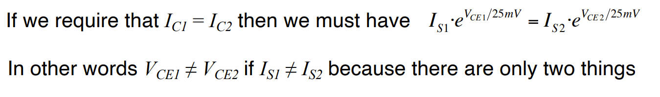
In general as our op amps are made from a long tail pair or something of the like (i.e more than one transistor by design), what we tend to find, is that the two comparative transistors for input arent identical. Which leads to a different in (perceived) input voltages at both terminals. Leading to a offset voltage:
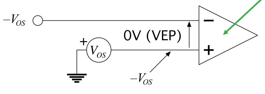
Generally Input Voltage Offset is very low, see: Example
Mitigating Offset
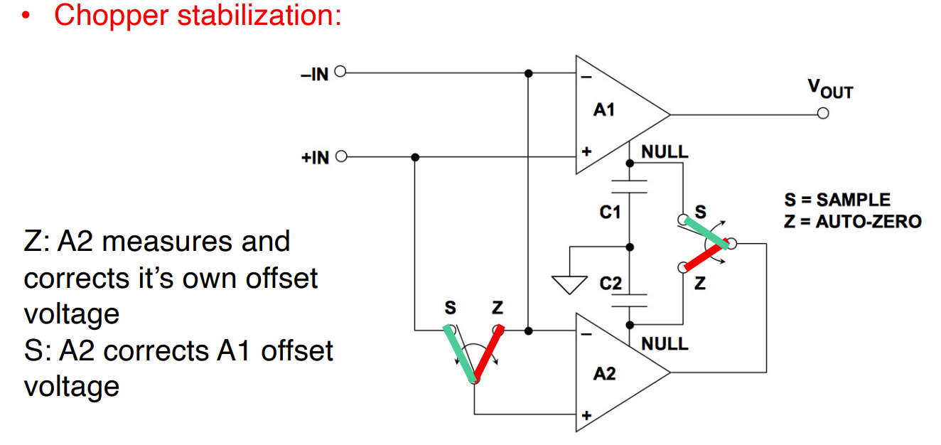
Chopper Stabilization:
Use for special occasions, not generally.
Benefits:
- MAX
- No 1/f noise (importartant todo)
- Compatible with Single Supp Operation
- Full Bandwidth Linear Amplification
- Massive DC gain
Problems:
- Dangerous
- Switching Noise, anywhere from 10-100kHz
- Could get beating from aligning frequencies of switching and actual signal
- If A1 is fully saturated, it leads to a horrible offset voltage in A2, and the recovery is very slow.
- Terrible performance above ~5kHz, useless for audio (Getting a LOT better quickly).
Graphical Example:
Representation on Circuit:
 7
7
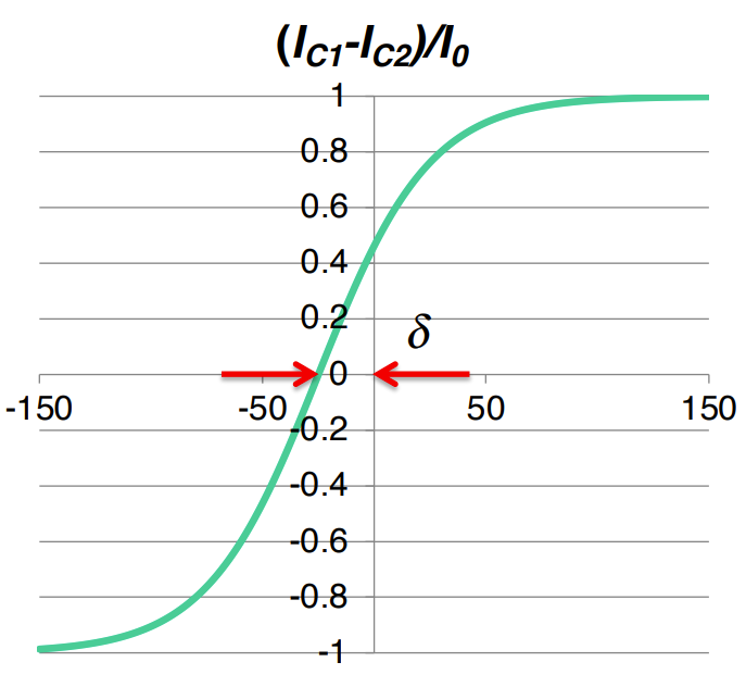
Offset Voltage Input Graph:
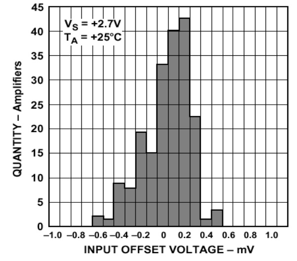 Standard Deviation of
In general, our specification state that our MAX offset is 6 * Standard Deviation. So here we can say that
Transclude of Voltage-Offset-2023-10-03-10.48.44.excalidrawOrder of conclusions drawn.