Tl;DR
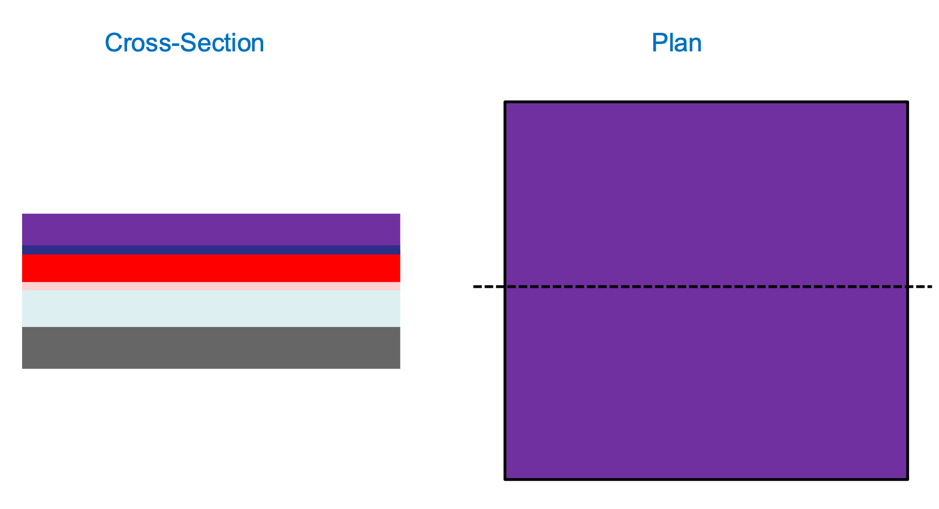
- Spin on resist
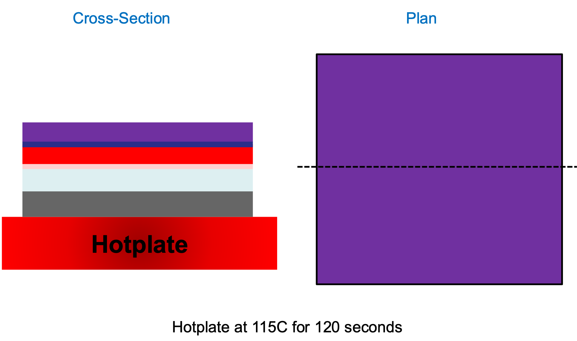
- Bake Resist
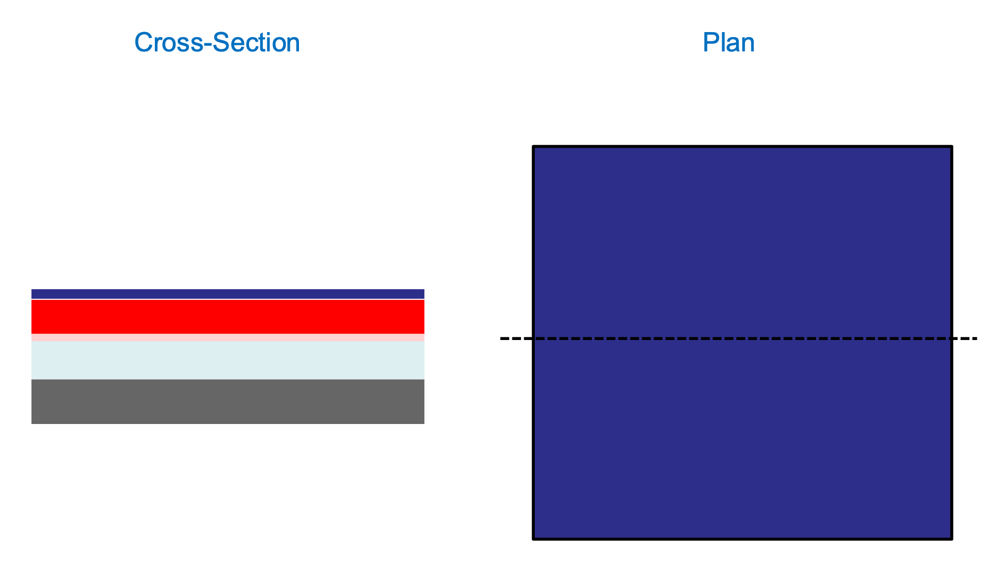
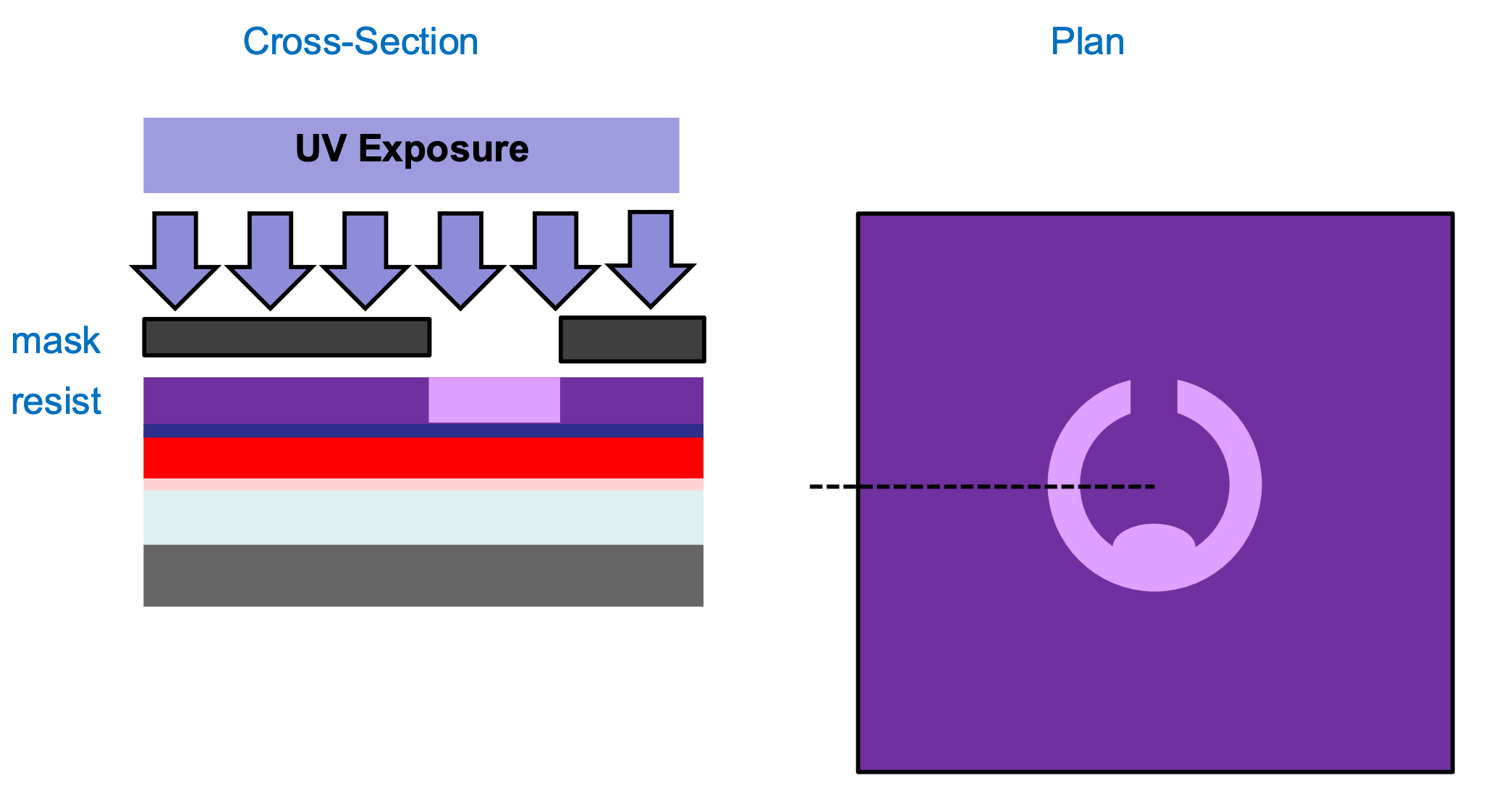
- Lithography of Contact Shape
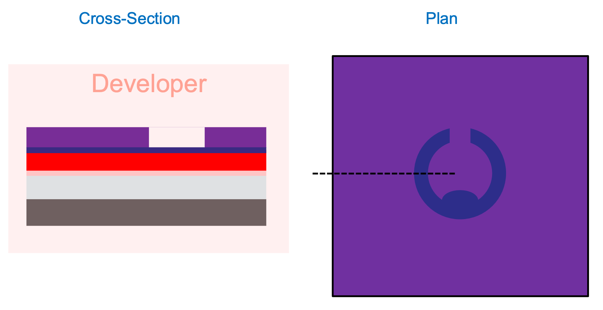
- Develop the resist out
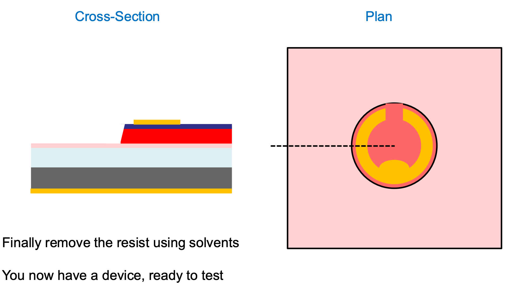
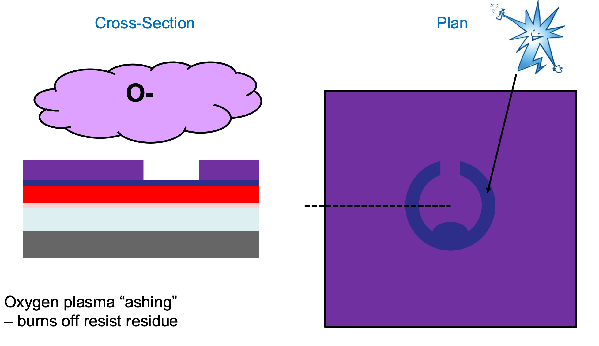
- “Ashing” resist residue
- p-contact metallisation (top)
- n-contact metallisation (bottom)
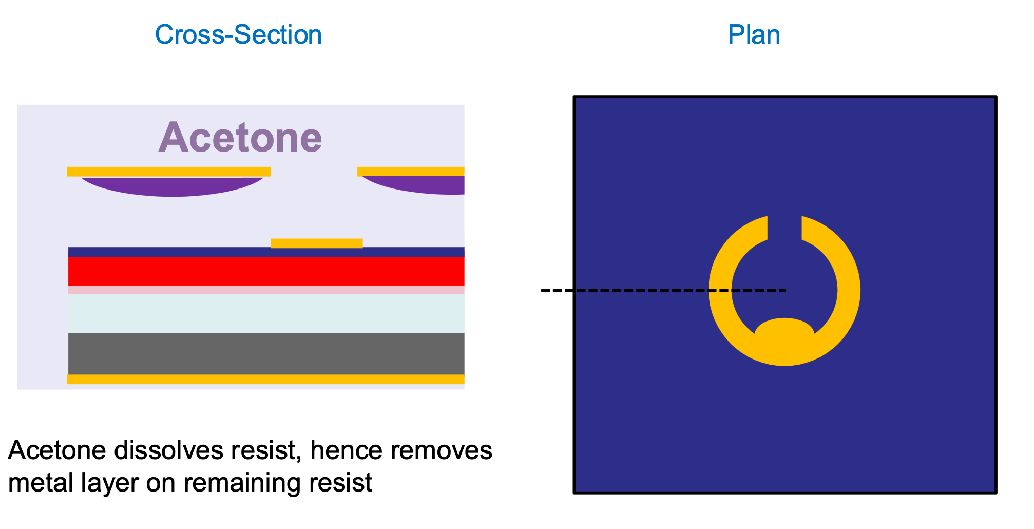
- Liftoff resist
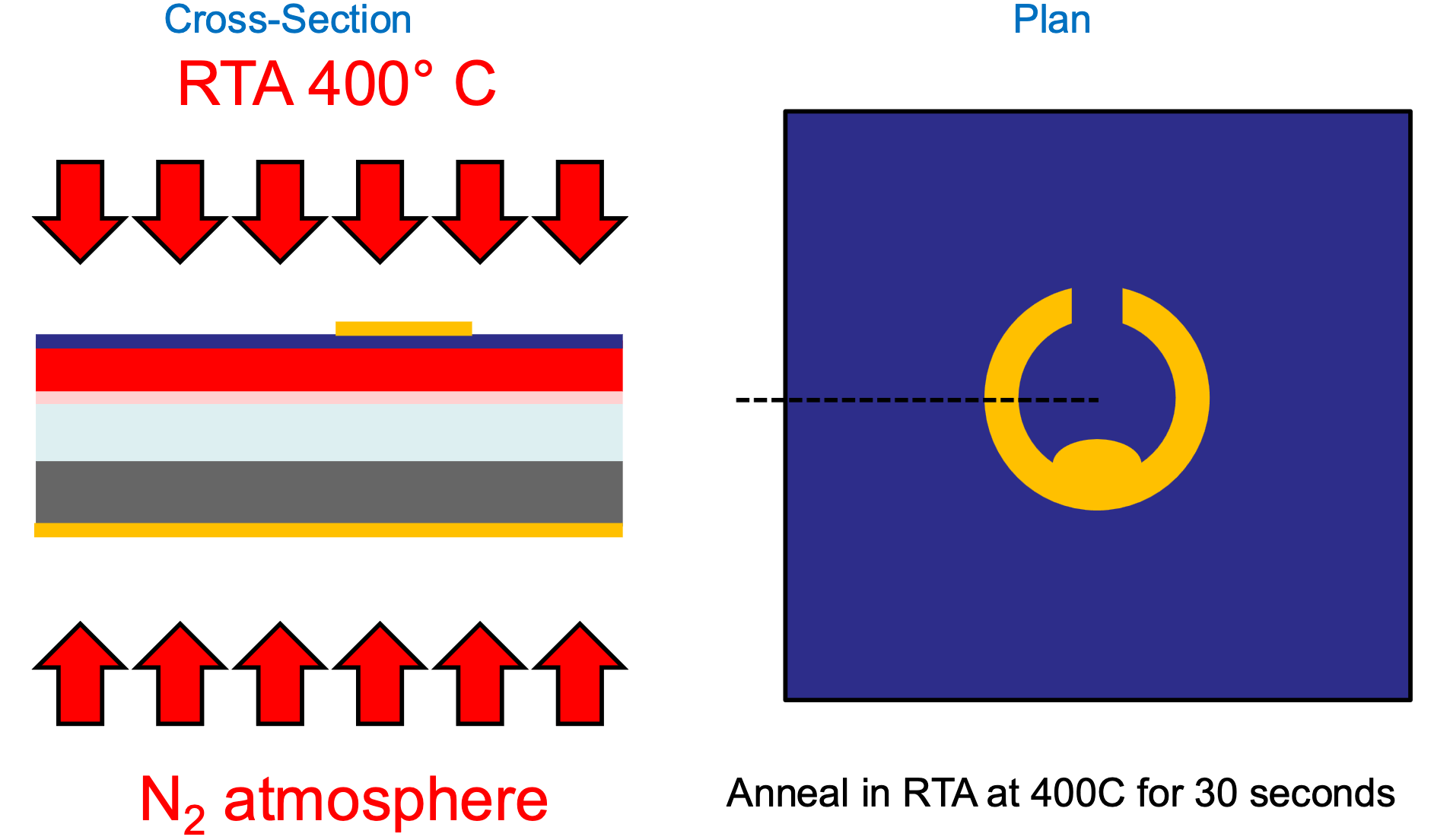
- Anneal contacts
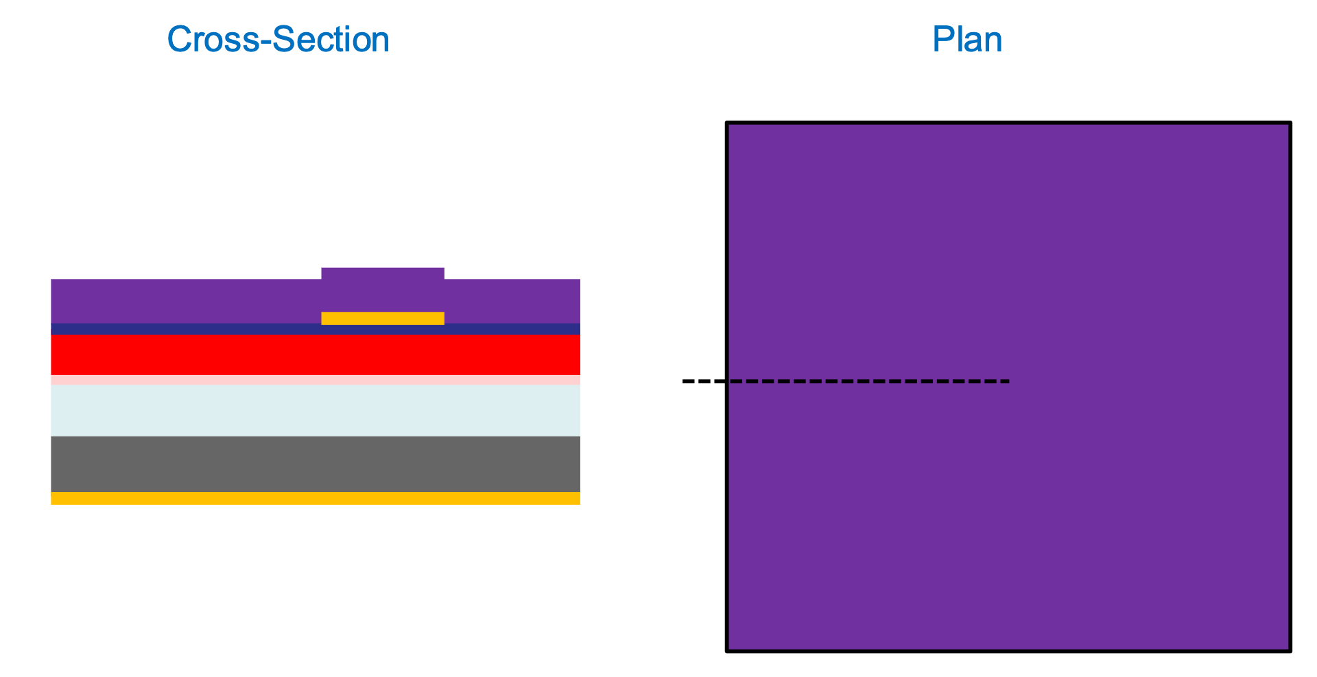
- Spin Resist
- Bake Resist
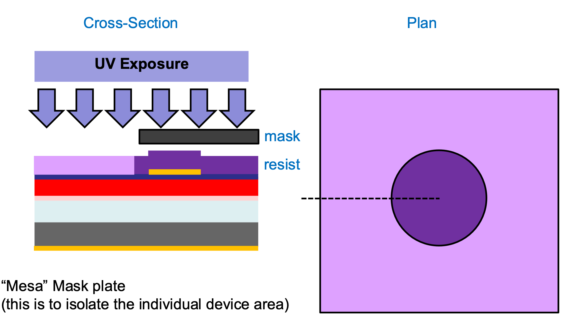
- Lithography of Mesa
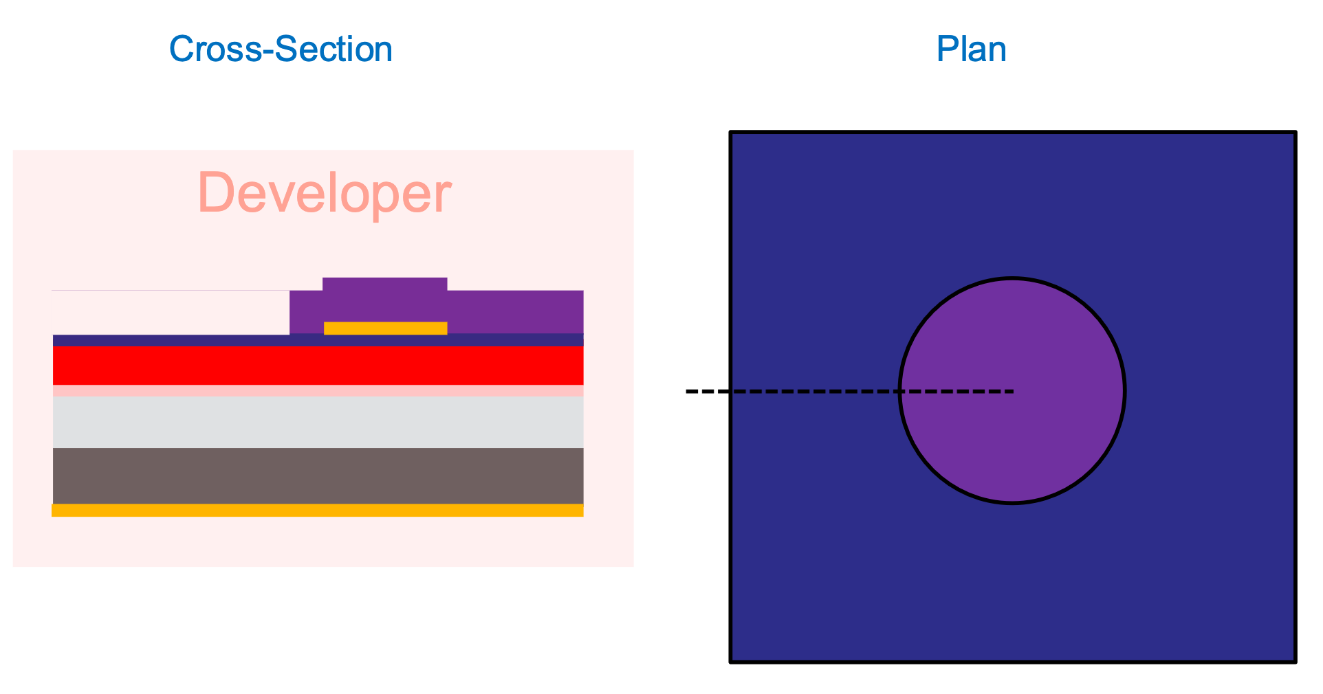
- Develop non-mesa resist
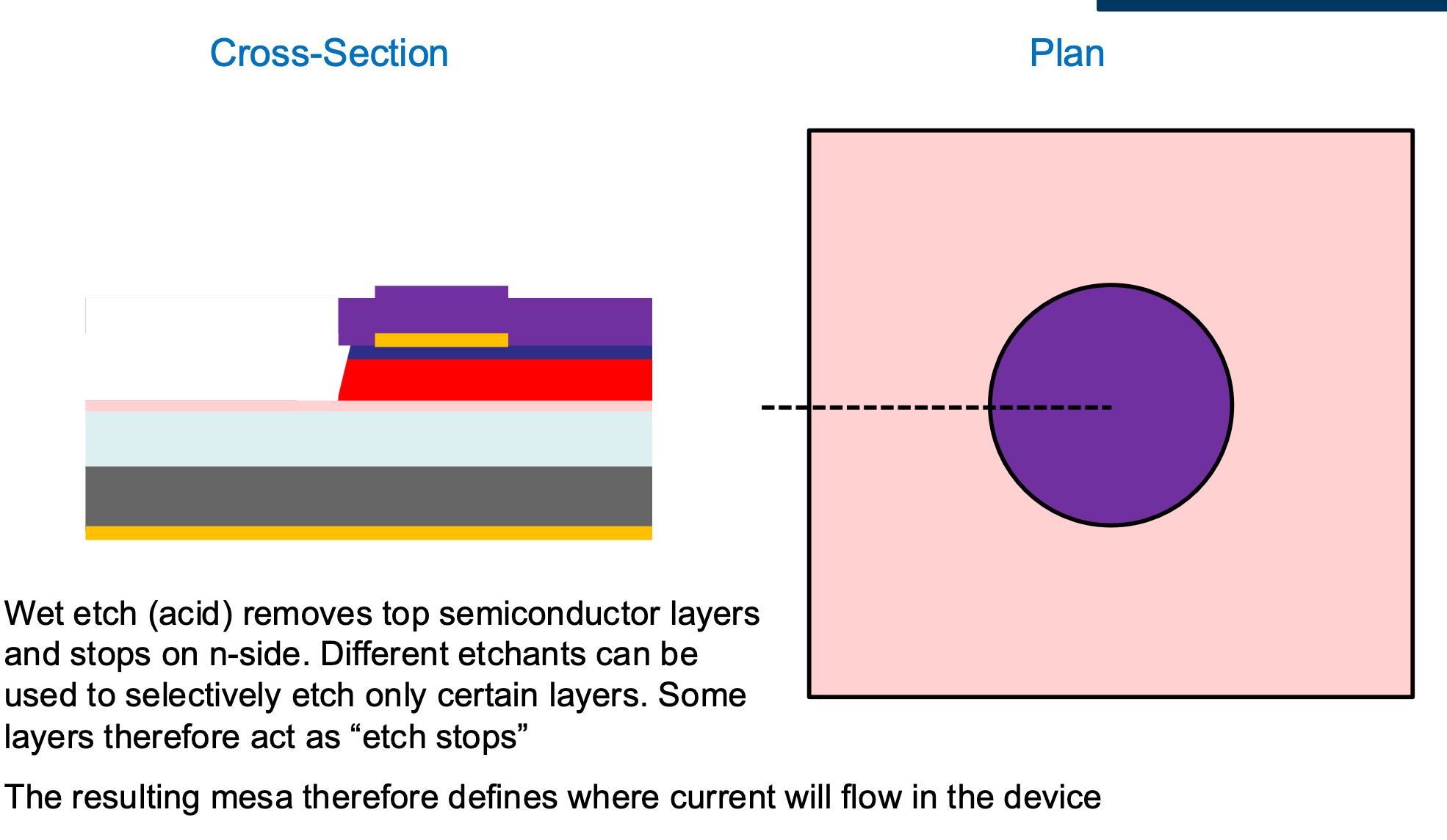
- Wet Etch down to n-side
- Strip Resist
Start with a virgin wafer:
| Layer | Thickness |
|---|---|
| p+ GaAs Contact | 150nm |
| p-AlInGaP | 1200nm |
| QW Layer (InGaP) | 200nm |
| n-AlInGaP | 1200nm |
| n+ GaAs Substrate | 550um |
Spin on resist:
Bake Resist
Lithography
Develop Contact Resist
Ashing Resist Residue
p-contact metallisation
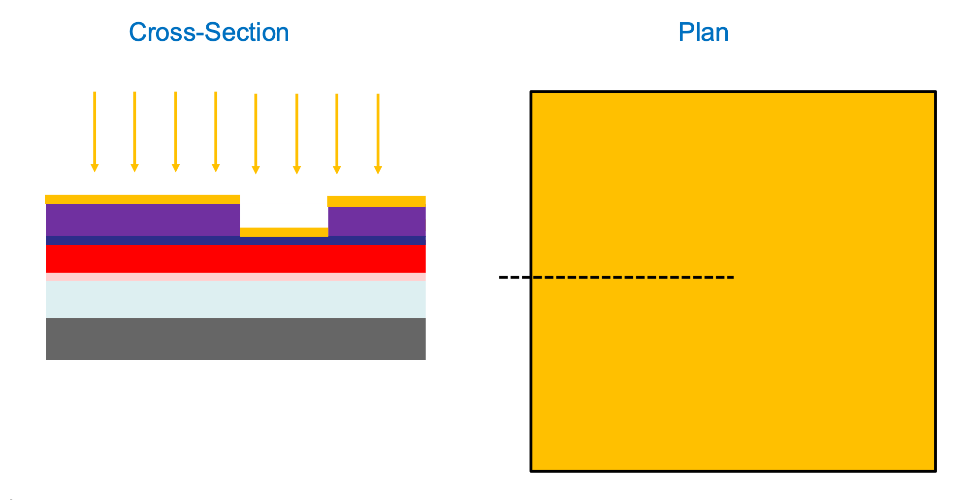 Ti/Au Alloy
n-contact metallisation
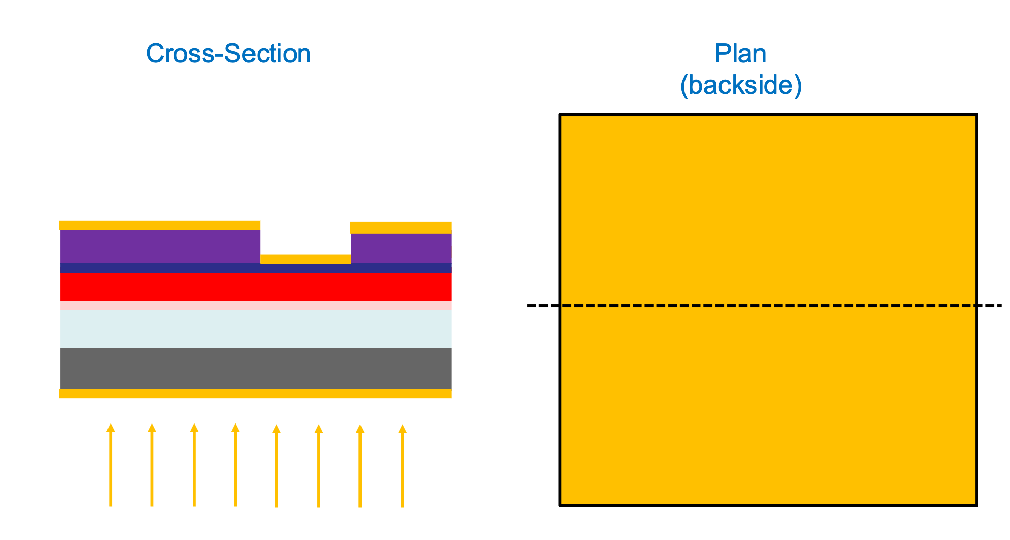 Ni/Au/Ge/Ni/Au Alloy
Liftoff Resist
Contact Annealing
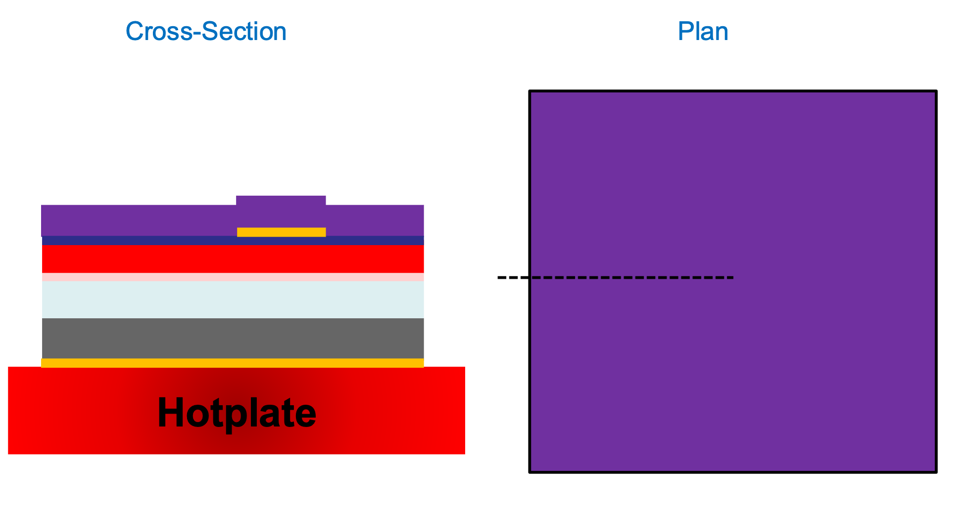
Spin Resist
Bake Resist
Lithography of Mesa
Develop Resist
Wet Etch
Strip Resist