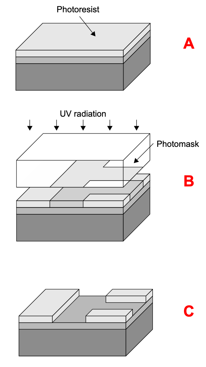
A -Prepare wafer, spin on photoresist (photosensitive chemical), bake B -Align photomask (transparent plate with chromium patterns) , expose with light (UV), bake C- Develop – in this case removes non-exposed regions (negative resist) D- Do something: Etch, deposit, diffuse, then remove remaining resist. Repeat until device completed
Positive vs Negative Photoresists
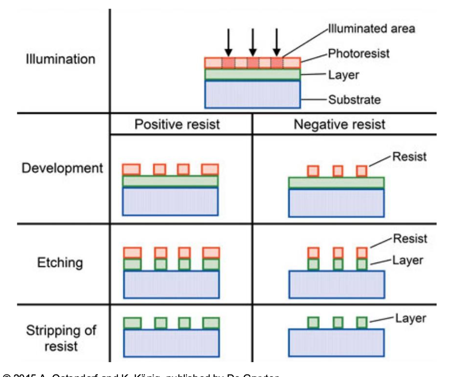
Positive resist: exposed resist becomes soluble to developer. Unexposed resist is insoluble. Unexposed areas remain.
Negative resist: exposed resist hardens and becomes insoluble to developer. Unexposed resist is soluble. Exposed areas remain.
| Property | Positive | Negative |
|---|---|---|
| Adhesion to Silicon | Fair | Excellent |
| Cost | More expensive | Less Expensive |
| Solubility in developer | Exposed region is insoluble | Exposed region is soluble |
| Min Feature | ||
| Step Coverage | Better | Lower |
| Wet Chemical Resistance | Fair | Excellent |
Spatial Resolution
Where $\lambda$ is the wavelength, $g$ is the gap width, $d$ is the resist thickness
![[Pasted image 20260420172648.png]]
Linewidth defines how well we can define features
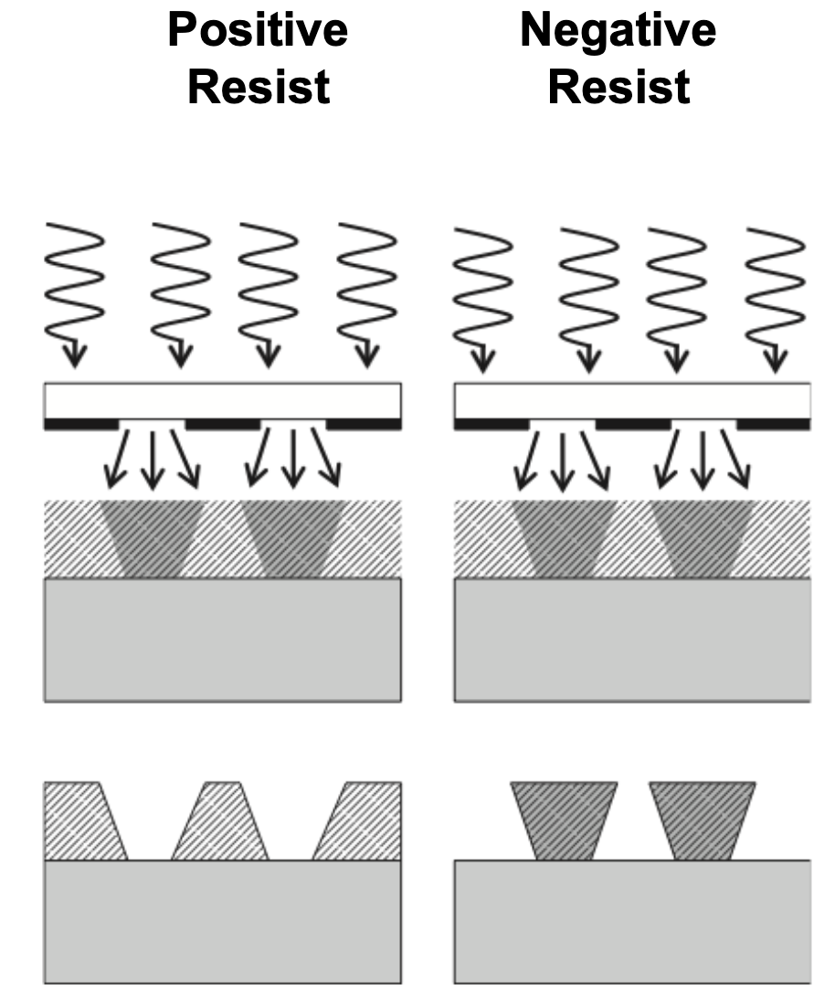
Resist Profiles
Binary & Phase Shift Masks
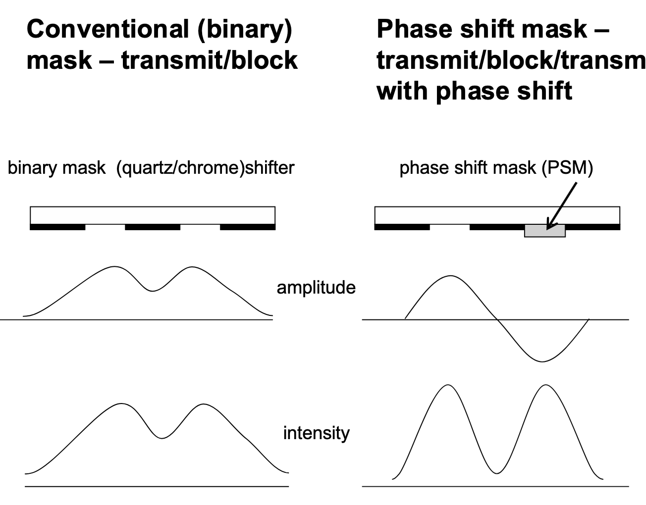
Phase shift mask uses interference effects to improve the contrast of the exposed and unexposed areas.
This can improve the resolution of the image on the wafer