Section A
1. Dry vs Wet Etching
Describe the relative advantages and disadvantages of wet etching and dry etching e.g. Reactive Ion Etching (RIE) [5]
Wet Etching:
- Isotropic (undercuts mask) — poor for fine features
- High selectivity — stops cleanly on etch-stop layers
- High throughput, low cost, simple
- Chemical waste disposal required
RIE (Dry):
- Anisotropic (directional ions) — vertical sidewalls, suitable for sub-micron features
- Lower selectivity than wet
- Plasma damage possible
- Slower, more expensive, lower throughput
- No liquid waste
2. Implantation
Sketch dopant concentration as a function of depth (z) for implantation into a i) single crystal and [5] ii) a single crystal with an amorphous surface coating. [2] You should clearly label any important features and comment on the advantages and disadvantages of each.
i) Single crystal:
- Gaussian-like profile peaked at projected range R_p
- Channelling can occur along crystal planes — atoms travel anomalously deep, producing a tail in the distribution beyond R_p
ii) Amorphous surface layer:
- The amorphous layer randomises ion trajectories before entering the crystal, suppressing channelling
- Peak still near R_p but sharper, more symmetric distribution
- Advantages: more predictable, controllable profile; no channelling tail
- Disadvantage: additional process step to deposit/grow amorphous layer; amorphous layer must later be removed or accounted for
3. Photoresist
Describe the difference between a positive and negative resist. Photo masks are made from quartz, with a thin layer of chromium on one side in which a pattern is etched.
i) Should the chrome side or quartz side be placed against the sample? [1] ii) Discuss why your resolution would be reduced if this was done incorrectly [2]
Positive resist: exposed regions become soluble and are removed — pattern transferred as-is from mask.
Negative resist: exposed regions cross-link and remain; unexposed regions removed — pattern is the inverse of the mask.
i) Chrome side should be placed against the sample.
ii) If quartz side faces the sample, there is a gap equal to the quartz thickness between the chrome pattern and the resist. Light diffracts as it passes through the quartz and around chrome edges, spreading before reaching the resist — this limits resolution. With chrome face-down, the pattern is in near-contact with the resist, minimising diffraction.
4. Proximity Effect
i) Describe the physical origin of the proximity effect in e-beam lithography. [2] ii) Explain how the proximity effect manifests itself. [2] iii) Explain how the proximity effect may be overcome. [1]
i) Physical origin: Primary electrons scatter within the resist and substrate. Forward scattering broadens the beam within the resist; back-scattering from the substrate returns electrons into surrounding resist over a much wider area (~several μm radius).
ii) Manifestation: Regions near densely written features receive additional dose from backscattered electrons — effectively over-exposed relative to isolated features. This causes pattern-dependent dimensional variation; closely spaced features merge or have incorrect critical dimensions.
iii) Overcoming it:
- Proximity effect correction (PEC): pre-calculate dose distribution and vary dose per feature to compensate
- Use a thinner resist (less forward scatter)
- Use a higher beam energy (forward scatter reduced, but backscatter range increases — net benefit in thin substrates)
- Use a low-Z substrate (less backscatter)
Section B
5. AFM Cantilevers
An AFM Silicon cantilever is formed by a beam of length l = 100 μm, width w = 10μm, and thickness t = 1 μm. The density of Silicon is 2330 kg/m3 and the Young’s modulus is E = 179 GPa. Calculate
Question
a) The mass of the cantilever. [2]
a) Mass:
Question
b) The spring constant for normal bending using the formula: . [2]
b) Spring constant:
Numerator:
Denominator:
Question
c) The resonance frequency (in Hz) of the cantilever associated with normal bending. [4]
c) Resonance frequency:
For a cantilever the effective mass is (standard result for first mode):
Question
d) The cantilever is operated at room temperature. Calculate the thermal rms deflection (the Boltzmann constant is kB ~ 10-23 J/K). [4]
d) Thermal rms deflection:
From equipartition:
This is sub-Ångström — consistent with AFM being sensitive to atomic-scale features.
Question
e) The five steps sketched below show snapshots in the process of manufacturing a freestanding AFM Silicon Nitride cantilever. Briefly describe the process necessary to go from a to b, b to c, c to d, and d to e. [8]
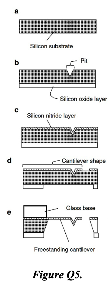
e) Fabrication steps (Figure Q5):
a → b: Anisotropic wet etch of the silicon substrate (e.g. KOH, which is crystallographically selective) to form a pit/recess. This defines where the cantilever tip will be.
b → c: Thermal oxidation or CVD to grow/deposit a silicon oxide layer conformally over the substrate surface including the pit. This acts as a sacrificial layer and etch stop.
c → d: LPCVD deposition of silicon nitride layer over the oxide. Photolithography and RIE to pattern the silicon nitride into the cantilever shape.
d → e: Anodic bonding of a glass base wafer to the underside. Wet etch (e.g. KOH) of the bulk silicon from beneath, stopping on the oxide; then HF etch to remove the sacrificial oxide — releasing the freestanding silicon nitride cantilever suspended over the glass base.
6. Temperature Accelerated Testing
In temperature accelerated life-testing, the mean time to failure (tf) is given by the following equation. Where k is the Boltzmann constant and T is temperature.
Question
a) Ea is an activation energy, explain the physical processes it represents in device failure. [2]
a) Physical meaning of E_a:
E_a is the energy barrier that must be overcome for the dominant failure mechanism to proceed — e.g. activation energy for electromigration, corrosion, or oxide breakdown. Thermally activated processes (governed by Arrhenius kinetics) require this energy to drive atomic diffusion, chemical reactions, or bond breaking that lead to device failure.
Question
b) Explain the processes, and assumptions made in order that temperature accelerated life-test may be carried out successfully. [4]
b) Process and assumptions:
- Devices are stressed at elevated temperatures T_high (accelerated) and the time to failure recorded
- Failures are assumed to follow the same mechanism at elevated T as at use T — critical assumption
- An Arrhenius plot of ln(t_f) vs 1/T is constructed; linearity confirms single-mechanism failure
- The slope gives E_a; extrapolation to use temperature gives predicted t_f
- Assumes failure mechanism, not just rate, is temperature-independent; assumes no new failure modes are triggered
Question
c) In temperature accelerated life-testing describe issues associated with using very high temperatures to speed up the lifetime assurance process. [2]
c) Issues with very high temperatures:
- New failure mechanisms activated at high T that don’t occur at use temperature — the Arrhenius extrapolation becomes invalid
- Phase changes, material interdiffusion, or melting of metallisation can occur
- Results no longer predict in-service behaviour — may be over- or under-optimistic
Question
d) If the mean time to failure of a component at a temperature of 150C is 200 hours, and Ea is 0.7eV, what is the mean time to failure at 50C? [6]
d) Mean time to failure at 50°C:
Convert temperatures: T₁ = 423 K, T₂ = 323 K, t_{f,1} = 200 hr
Question
e) Comment on the application of this approach to other forms of fatigue. [2]
e) Application to other fatigue types:
The Arrhenius approach applies to any thermally activated failure mechanism. It has been extended to electromigration (Black’s equation), humidity-accelerated corrosion (Peck’s model), and voltage-accelerated oxide breakdown. However, mechanical fatigue (cyclic stress) and vibration fatigue are not thermally activated in the same way — different acceleration models (e.g. Coffin-Manson) are more appropriate. Combined stresses (HALT/HASS testing) attempt to cover multiple mechanisms simultaneously.
Question
f) Figure Q6 shows a mask pattern and an electron micrograph after the photolithography process. The original pattern consists of tapered lines 15 μm wide (at their widest end) of 200-300 μm length. Describe possible modes of failure of this process, and how this problem may be rectified. [4]
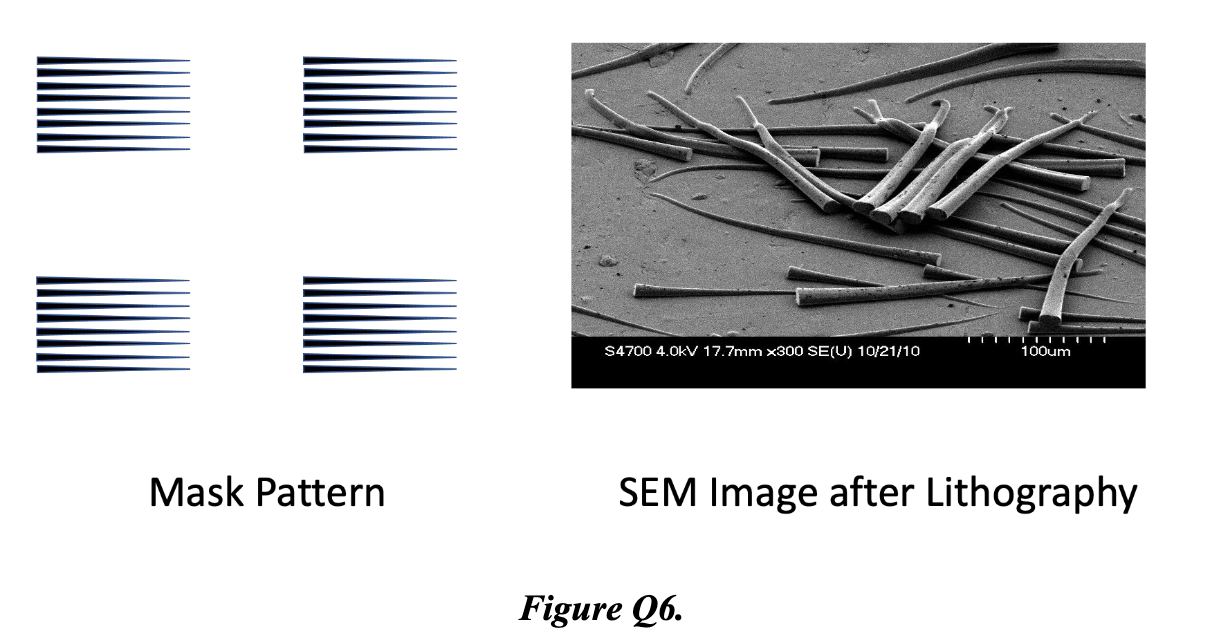
f) Lithography failure modes (Figure Q6):
The SEM shows the narrow tapered lines have collapsed and are lying flat on the substrate rather than standing. Failure modes:
- Resist collapse: high aspect ratio lines (narrow width relative to resist thickness) are mechanically unstable — surface tension during development pulls them over
- Adhesion failure: poor resist-substrate adhesion at the narrow tip causes delamination
- Undercutting: isotropic etch component undercuts the base
Rectification:
- Reduce resist thickness to lower aspect ratio
- Use supercritical CO₂ drying instead of solvent rinse to eliminate surface tension during development
- Apply adhesion promoter (e.g. HMDS)
- Optimise exposure/development to reduce undercut
7. Damascene process
Question
a) Explain the historical motivation for the introduction of the Damascene process (copper interconnects) in integrated circuit manufacture. [4]
a) Historical motivation:
As device scaling continued into the sub-0.25 μm node, aluminium interconnect RC delay became the dominant performance limiter — resistance of narrow Al lines increased substantially. Copper has ~40% lower resistivity than Al. Additionally, Cu has superior electromigration resistance. The challenge was that Cu cannot be dry etched cleanly (no volatile Cu etch products at room temperature), necessitating a fundamentally different patterning approach.
Question
b) What different process steps and procedures were required in the Damascene process as compared to standard aluminium interconnect processes? [6]
b) New process steps vs Al:
| Step | Al process | Damascene |
|---|---|---|
| Metal deposition | PVD Al blanket | Electroplated Cu into pre-etched trenches |
| Patterning | Etch metal through mask | Etch dielectric; metal fills trenches |
| Planarisation | Not required | CMP essential to remove overburden Cu |
| Barrier layer | Not typically needed | TaN/Ta barrier required (Cu diffuses into Si/SiO₂) |
| Dielectric | SiO₂ | Low-k dielectrics used for further RC reduction |
Dual Damascene integrates via and trench in a single fill step.
Question
c) Describe, with schematics, if necessary, the metallization lift-off process. [4]
c) Metallisation lift-off:
- Deposit resist on substrate; pattern by lithography — openings where metal is wanted
- Key requirement: resist profile must be re-entrant (undercut) — wider at base than top, achieved by using image reversal resist or a bilayer resist stack
- Deposit metal by directional PVD (e-beam evaporation) — metal lands on open substrate and on top of resist, but does not coat the undercut sidewalls
- Soak in solvent (acetone) — resist dissolves, lifting off the metal on top; metal in the openings remains
Substrate → Resist (undercut) → Metal deposition → Lift-off
Question
d) Explain how this process may fail, possible reasons for the failure, and how such failure can be avoided. [6]
d) Lift-off failure modes:
- Continuous metal film (no undercut): metal bridges across resist sidewalls — solvent cannot access resist; metal tears rather than lifts cleanly → ensure re-entrant profile
- Resist dissolution by metal deposition heat: use e-beam rather than sputtering (lower substrate heating); keep deposition rate moderate
- Metal adhesion too high: residue remains after lift-off → use appropriate solvent and ultrasonic agitation
- Incomplete lift-off of thick films: keep metal thickness well below resist thickness (typically metal < 1/3 resist thickness)
Section C
8. Antireflection coating
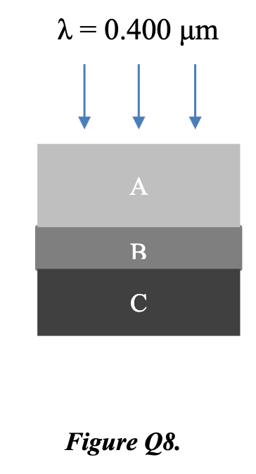
A structure is a made of a sequence of three layers A/B/C. A and C are thick layers of index of refraction nA = 1.33 and nC = 3.00, respectively. B is a thin layer of index of refraction nB, designed to eliminate reflected light at wavelength (in air) of 0.400 μm when incident normally as in figure Q8.
You have four possible choices for B:
- Leave a gap of air nB = 1.00.
- A metal with (the real part of the index of refraction equal to) nB =1.66.
- A dielectric with nB = √3.
- A dielectric with nB = 2.
Question
a) Describe, with reasoning, the best choice for material B from these options. [4]
a) Best choice for material B:
For zero net reflection, two conditions must both be satisfied:
-
Amplitude condition: reflected amplitudes from A/B and B/C interfaces must be equal → requires
-
Phase condition: the two reflections must be 180° out of phase. Since , both reflections involve going from lower to higher index → both get a π phase shift on reflection. The additional path difference of 2n_B·d must therefore equal λ/2, i.e. quarter-wave thickness.
-
Material must be a dielectric — a metal has complex refractive index, causing absorption and additional phase shifts that prevent complete cancellation.
Best choice: n_B = 2 (dielectric, satisfies amplitude condition exactly)
n_B = √3 ≈ 1.732 ≠ 2.00 — amplitude condition not met; n_B = 1.00 and 1.66 also fail.
Question
b) For your selected material for B, what is the thickness, d, that realizes the best antireflecting coating? [6]
b) Required thickness:
Quarter-wave condition in medium B:
where λ = 0.400 μm (in air):
Question
c) In this process, if layer C is a substrate wafer, and you want to check if the thickness of B is correct before depositing A, describe approaches you would use to assure this thickness. Discuss destructive and non-destructive processes, and manufacturing procedures that could be employed. Indicate the advantages and disadvantages of the methods you suggest. [10]
c) Thickness verification methods:
Non-destructive:
-
Ellipsometry: measure change in polarisation state of reflected light. Fits n and d simultaneously with sub-nm precision. Fast, non-contact, industry standard. Requires accurate optical model of the material.
-
Reflectometry: measure reflectance spectrum vs wavelength. Interference fringes give thickness directly. Simpler than ellipsometry but less precise for very thin films.
-
In-situ optical monitoring during deposition: real-time reflectance at λ = 400 nm reaches a minimum at quarter-wave thickness — can halt deposition at the minimum. Fast, zero additional metrology step; assumes optical constants are well known.
Destructive:
-
Cross-section TEM/SEM: physically cleave and image the cross-section. Direct, high-resolution measurement. Destroys the sample — only used on witness/test wafers.
-
Profilometry with etch step: mask and etch through the film, measure step height with a stylus profilometer. Damages the measured area — acceptable on test structures at wafer edge.
Manufacturing procedures:
- Deposit on monitor/witness wafers alongside product wafers and measure these
- Use statistical process control (SPC) on deposition rate × time to control thickness between metrology points
- In-situ endpoint detection (reflectance minimum) eliminates the need for post-deposition metrology
9. Dry etching
Question
(a) What are the typical reactions that occur on a sample surface during dry etching? Your answer should provide a brief description of each. [8]
a) Surface reactions:
- Physisorption: neutral radicals and etchant species adsorb weakly onto the surface — precursor to chemical reaction
- Chemisorption: species form chemical bonds with surface atoms — reactive neutrals (e.g. F radicals on Si form Si-F bonds)
- Chemical etching: adsorbed radicals react with surface to form volatile products (e.g. SiF₄) which desorb — purely chemical, isotropic
- Ion bombardment / sputtering: energetic ions physically eject surface atoms by momentum transfer — purely physical, anisotropic, low selectivity
- Ion-assisted chemistry: sub-threshold ions activate chemisorbed species, greatly enhancing chemical etch rate at the surface only — this synergistic mechanism gives RIE its anisotropy with reasonable selectivity
- Redeposition: sputtered material or non-volatile by-products redeposit on sidewalls — can cause micromasking or residue
Question
(b) What affect does reducing the pressure have on plasma? How would this affect the dry etch? [4]
b) Effect of reducing pressure:
Lower pressure → longer mean free path → ions undergo fewer collisions in the sheath → arrive at the wafer with greater energy and more directionality. This increases anisotropy and ion energy. However, radical density also decreases, reducing the chemical etch component. Net effect: etch becomes more physical/sputter-like — higher aspect ratio capability but lower selectivity and increased ion damage.
Question
(c) What is meant by the term ‘dry etch damage’, what are its typical causes and what measures can be taken to minimise it? [4]
c) Dry etch damage:
Energetic ion bombardment displaces lattice atoms, creating point defects (vacancies, interstitials) and broken bonds in the near-surface region — this is etch damage. UV photons from the plasma also cause interface state generation in gate oxides.
Causes: high ion energy, high ion flux, prolonged exposure.
Minimisation:
- Reduce bias voltage (lower ion energy)
- Use high-density low-pressure plasma (ICP) which decouples ion flux from ion energy — maintain flux while reducing energy
- Post-etch anneal to recover lattice damage
- Sacrificial etch stop layer absorbs damage
Question
(d) Other undesirable effects in a dry etch are ‘loading effects’ and ‘non-uniformity’. How do these phenomena differ from each other, and can they be resolved by employing a dry etch tool with a larger etch chamber? Your answer should include details on the underlying mechanisms for each phenomenon. [4]
d) Loading effects vs nonuniformity:
Loading effect: global — etch rate depends on total amount of material being etched across the entire chamber. With more exposed etchable area, reactant is consumed faster → etch rate drops. Mechanism: reactant depletion. Larger chamber doesn’t help — it increases the volume of gas but doesn’t change the reactant consumption rate per unit area.
Nonuniformity: spatial — etch rate varies across a single wafer or between wafers at different positions in the chamber. Caused by non-uniform plasma density, gas flow distribution, or temperature gradients. Larger chamber may worsen centre-to-edge nonuniformity unless plasma and gas delivery are redesigned to match.
They are distinct: loading is a global rate effect; nonuniformity is a spatial distribution effect. A larger chamber resolves neither without accompanying redesign of gas injection and plasma confinement.
10. Diffusion
Question
a) Equation Q10 permits the calculation of the diffusion coefficient for a dopant in a semiconductor.
i. What does the activation energy (Ea) tell us about the underlying diffusion process? [2] ii. Temperature (T in equation 10) plays a significant role in diffusion. What impact does its relationship with the diffusion coefficient have on how we design a) diffusion furnaces and b) annealing systems? [5]
a) i) Activation energy E_a:
E_a quantifies the energy barrier a dopant atom must overcome to move to an adjacent site. It reflects the strength of the bonds that must be broken and the lattice strain involved in the jump. A high E_a means diffusion is strongly temperature-dependent and negligible at low T; a low E_a means appreciable diffusion even at moderate temperatures.
a) ii) Impact of T on furnace/annealer design:
Since , D is extremely sensitive to T. A small temperature variation ΔT gives a large variation in D and therefore in junction depth:
- Diffusion furnaces must maintain highly uniform temperature along the tube (±0.5°C or better) using multi-zone heating with independent PID control; ramp rates must be slow and controlled to prevent slip dislocations from thermal shock
- Annealing systems (e.g. RTA for dopant activation after implant) must have precisely controlled ramp-up and soak time — short high-T anneal activates dopants with minimal diffusion; temperature overshoot would cause unacceptable junction movement; lamp-based RTA systems with pyrometry feedback used for fast, precise control
Question
(b) Explain what is meant by i) interstitial and ii) vacancy diffusion processes. Which, if any, of the terms you described in a) change between i) interstitial and ii) vacancy diffusion and what does this tell us about each process. You may wish to employ sketches to help your explanation. [5]
b) Interstitial vs vacancy diffusion:
-
Interstitial: dopant atom jumps through interstitial sites between host lattice atoms. No host atom displacement needed. Low E_a, high D, fast. Typical for small atoms (Li, H, Cu in Si).
-
Vacancy: dopant atom moves into an adjacent vacancy in the host lattice. Requires both a vacancy to be present and the atom to have sufficient energy to jump. Higher E_a, slower. Typical for substitutional dopants (B, P, As in Si).
Between the two: D₀ (pre-exponential) and E_a both change. D₀ encodes the attempt frequency and geometry of the jump; E_a encodes the barrier. Interstitial diffusion has lower E_a and larger D₀ for small atoms; vacancy diffusion has higher E_a reflecting the vacancy formation and migration energies.
Question
(c) How do i) constant surface concentration diffusion and ii) constant total dopant diffusion differ from each other? Your answer should include specific scenarios where each one is relevant [4]
c) Constant surface concentration vs constant total dopant:
Constant surface concentration (predeposition / erfc profile):
- Surface concentration C_s held fixed (e.g. by maintaining dopant atmosphere in furnace)
- Total dopant in wafer increases with time
- Used for: initial doping from a gas/solid source; forming heavily doped surface regions
Constant total dopant (drive-in / Gaussian profile):
- Total dopant Q fixed (implanted dose or predeposited layer)
- Surface concentration decreases as dopant spreads deeper with time
- Used for: redistribution of a fixed implanted dose; junction depth control after implant
Question
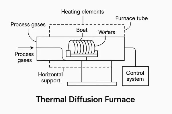
d) Draw a sketch of a basic diffusion furnace, labelling the important features. [4]
d) Basic diffusion furnace sketch:
 Gas inlet (dopant source + carrier)
       |
  [  MFC  ]
       |
  _____|_______________________________________
 |     |                                      |
 |  →→→→→→→→→→→→→→→→→→→→→→→→→→→   quartz tube |
 |     [wafers on quartz boat]                |
 |  [zone 1] [zone 2] [zone 3]                |
 |  [ heat ] [ heat ] [ heat ]                |
 |____________________________________________|
                                    |
                              exhaust / scrubber

Key features:
- Multi-zone resistance heating (independent PID per zone)
- Quartz process tube
- Quartz wafer boat
- Thermocouple at each zone
- Mass flow controllers on all gas lines
- Exhaust scrubber (toxic dopant gases)
- Slow push/pull mechanism for wafer loading