Constants:
- c = 3.00×10⁸ m s⁻¹ | e = 1.60×10⁻¹⁹ C | h = 6.63×10⁻³⁴ J s
- k_B = 1.38×10⁻²³ J K⁻¹ | ε₀ = 8.85×10⁻¹² F m⁻¹
Section A [20 marks]
Question
- Describe the relative advantages and disadvantages of wet etching and dry etching e.g. Reactive Ion Etching (RIE). [5]
Question
Sketch dopant concentration as a function of depth (z) for implantation into a:
- i) single crystal [5]
- ii) single crystal with an amorphous surface coating [2]
Clearly label any important features and comment on the advantages and disadvantages of each.
Question
Describe the difference between a positive and negative resist. Photo masks are made from quartz with a thin chromium layer on one side in which a pattern is etched.
- i) Should the chrome side or quartz side be placed against the sample? [1]
- ii) Discuss why resolution would be reduced if this was done incorrectly. [2]
4. Regarding the proximity effect in e-beam lithography:
- i) Describe its physical origin. [2]
- ii) Explain how it manifests itself. [2]
- iii) Explain how it may be overcome. [1]
Section B [40 marks]
Question
An AFM Silicon cantilever has length l = 100 μm, width w = 10 μm, thickness t = 1 μm. Silicon density = 2330 kg/m³, Young’s modulus E = 179 GPa.
- a) Calculate the mass of the cantilever. [2]
- b) Calculate the spring constant for normal bending using k_N = (E w t³)/(4l³). [2]
- c) Calculate the resonance frequency (Hz) associated with normal bending. [4]
- d) The cantilever is operated at room temperature. Calculate the thermal rms deflection (k_B ≈ 10⁻²³ J/K). [4]
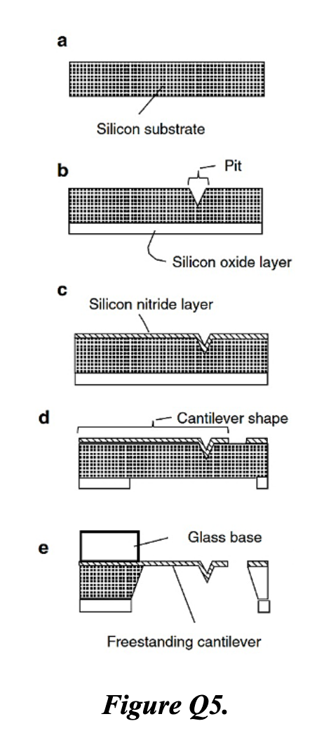
- e) The five steps below show snapshots in manufacturing a freestanding AFM Silicon Nitride cantilever. Briefly describe the process to go from a→b, b→c, c→d, and d→e. [8]
(See Figure Q5: silicon substrate → pit formation → silicon oxide layer → silicon nitride layer → cantilever shape definition → freestanding cantilever on glass base)
Question
In temperature accelerated life-testing, mean time to failure is given by: where k is Boltzmann’s constant and T is temperature.
- a) Explain the physical processes the activation energy E_a represents in device failure. [2]
- b) Explain the processes and assumptions required to carry out a temperature accelerated life-test successfully. [4]
- c) Describe issues associated with using very high temperatures to speed up the lifetime assurance process. [2]
- d) If mean time to failure at 150°C is 200 hours and E_a = 0.7 eV, calculate the mean time to failure at 50°C. [6]
- e) Comment on the application of this approach to other forms of fatigue. [2]
- f) Figure Q6 shows a mask pattern and SEM image after photolithography. The original pattern consists of tapered lines 15 μm wide (at widest) of 200–300 μm length. Describe possible modes of failure and how they may be rectified. [4]
7. Regarding the Damascene process:
- a) Explain the historical motivation for introducing the Damascene process (copper interconnects) in IC manufacture. [4]
- b) What different process steps and procedures were required in the Damascene process compared to standard aluminium interconnect processes? [6]
- c) Describe, with schematics if necessary, the metallisation lift-off process. [4]
- d) Explain how this process may fail, possible reasons for failure, and how such failure can be avoided. [6]
Section C [40 marks]
Question
- A structure comprises three layers A/B/C. A and C are thick layers with refractive indices n_A = 1.33 and n_C = 3.00. B is a thin layer of index n_B designed to eliminate reflected light at λ = 0.400 μm (in air) under normal incidence.
Possible choices for B:
Air gap: n_B = 1.00
Metal: n_B = 1.66
Dielectric: n_B = √3
Dielectric: n_B = 2
a) Describe, with reasoning, the best choice for material B. [4]
b) For your selected material, calculate the thickness d that realises the best antireflecting coating. [6]
c) If layer C is a substrate wafer and you want to verify the thickness of B before depositing A, describe approaches you would use. Discuss destructive and non-destructive processes and manufacturing procedures, including advantages and disadvantages of each. [10]
9. Regarding dry etching:
- a) What are the typical reactions that occur on a sample surface during dry etching? Provide a brief description of each. [8]
- b) What effect does reducing pressure have on plasma, and how does this affect the dry etch? [4]
- c) What is meant by ‘dry etch damage’, what are its typical causes, and what measures minimise it? [4]
- d) How do ‘loading effects’ and ‘nonuniformity’ differ from each other, and can they be resolved by using a larger etch chamber? Include the underlying mechanisms for each. [4]
10. The diffusion coefficient for a dopant in a semiconductor is given by Equation Q10.
- a)
- i) What does the activation energy E_a tell us about the underlying diffusion process? [2]
- ii) What impact does temperature’s relationship with the diffusion coefficient have on the design of a) diffusion furnaces and b) annealing systems? [5]
- b) Explain interstitial and vacancy diffusion processes. Which terms from (a) change between the two, and what does this tell us about each process? [5]
- c) How do constant surface concentration diffusion and constant total dopant diffusion differ? Include specific scenarios where each is relevant. [4]
- d) Draw a labelled sketch of a basic diffusion furnace. [4]