Attempt ALL of Section A, any TWO from Section B, and any TWO from Section C.
Constants: c = 2.997×10⁸ m/s | h = 6.626×10⁻³⁴ J/s | e = 1.602×10⁻¹⁹ C | m_e = 9.109×10⁻³¹ kg | k_B = 1.381×10⁻²³ J/K
Section A [20 marks]
Question
- Give reasons for the use of reflecting mirrors instead of lenses in photolithography. [5]
Mirrors aren’t affected by Chromatic abberation, as that is dependant on the difference wavelength has on refracation, not reflection.
Mirrors also can be used in succession without as severely magnifying the problem of spherical abberations, and flat mirrors dont face this issue at all
2. What is meant by 'loading effects' in dry etching? Your answer should include two types, describing their mechanism and impact on the resulting etch. [5]
Loading effects refer to the general effect the total etchable area has on the etch rate, and micro-laoding effects are related to the specific aspect ratio of each etchable region. Loading effects can ruin calculations of etch time needed for certain depths, where micro-loading has the issue where larger etching regions (lower aspect ratio) will have different etch depths for the same etch time as smaller regions
3. What is the ideal concentration distribution of an implanted dopant region? What is channelling and why does it disrupt the ideal profile? Give one strategy to prevent it. [5]
the ideal concentration distribution is a gaussian curve with its peak shifted slightly deeper into the material. Channelling occurs when ions approach at a certain angle, inbetween atoms, and are effectively forced into a channel in the repetitive crystal lattice, until they eventually are slowed enough to be pulled into a stop. This leads to ions being much deeper than they should, and adds a tail to the right hand side of the gaussian distribution. We can prevent this by adding a small amorphous layer to the surface, effectively preventing ions getting into these channels in the lattice in the first place.
4. Describe schematically the process flow steps for the Damascene process for interconnect metallisation. [5]
The damascene process has you first deposit a negative resist layer, expose the regions where you want the metal to go, deposit a uniform layer of copper across the entire surface, then polish the excess until you reach the resist, where you then expose the rest of the resist and remove.
Section B [40 marks]
5. An SEM can accelerate electrons at V = 1 kV, 5 kV, and 10 kV, and has SED, BSD, and EDS detectors.
- a) Determine the de Broglie wavelength of an electron accelerated through V = 1 kV and V = 10 kV. Ignore relativistic corrections. [5]
- b) What V and detector combination best images the elemental composition of Sample A (atomically flat, mixed microcrystals)? [5]
- c) What V and detector combination best images the surface details of the gold particles on Sample B? [5]
- d) What V and detector combination best measures the diameter of the 220 nm tall, ~20 nm diameter SiO₂ pillars on Sample C? [5]
a)
b) EDS radiaiton, 10kV. We need high voltage to penerate deep enough to get the X-rays which are perfect for detecting radiation
c) SE 1kV, to avoid putting too much energy into the conductive gold, as well as to just get the surface details
d) SE 5kV, slightly higher to get between the pillars, but still only observing the surface
6. Growing SiO₂ on ⟨100⟩ silicon.
- a) Using the graph, estimate the time to grow 200 nm at 1100°C in dry oxygen. [2]
- b) The wafer is then put in wet oxygen at 1000°C. Using the graph, how long to grow an additional 300 nm? [8]
- c) Repeat part (b) analytically using oxidation theory and Table 1. [10]
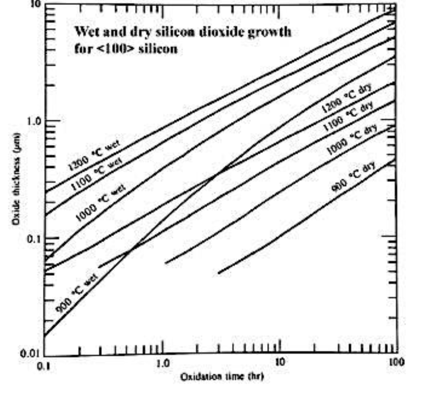
a) 4hrs b) 0.5hrs → 1.5hrs = 1hrs
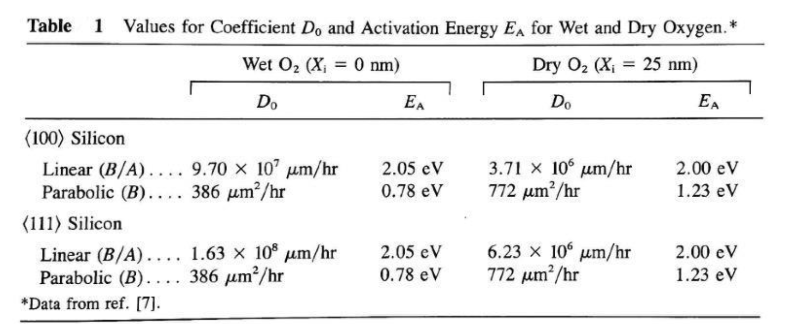
c) From Table 1, wet O₂, ⟨100⟩:
- B/A: D₀ = 9.70×10⁷ μm/hr, E_A = 2.05 eV
- B: D₀ = 386 μm²/hr, E_A = 0.78 eV
At T = 1000°C = 1273 K, k_BT = (8.617×10⁻⁵)(1273) = 0.1097 eV
7. Optical lithography and lift-off.
- a) Describe the key concepts behind contact optical lithography, using schematics where appropriate. [6]
- b) With reference to the linewidth formula, describe strategies to minimise feature size. [5]
- c) Describe a suitable photoresist profile to achieve 500 nm thick, 3 μm wide metal stripes on a 300 μm period via lift-off. Use schematics if necessary. [3]
- d) Describe possible failure modes for the above lift-off process and how you would identify them. [6]
Section C [40 marks]
8. Test structures and characterisation.
- a) Figure Q8 shows three common test structures.
- i) Identify the characterisation technique associated with each. [3]
- ii) Briefly describe how each technique is performed. [9]
- iii) Detail the information extractable from each. [5]
- b) Draw a schematic of the forward I-V characteristics of a p-n diode with and without additional series resistance from a non-ideal contact. [3]
9. Wet etching.
- a) Some wet etches generate bubbles. Why are they generated, and how do they cause fabrication problems? Include a sketch illustrating the mechanism. [7]
- b) Why is the Arrhenius relationship important for wet etch controllability, and how can its principles be used to improve control? [5]
- c) Why can thin surface contamination layers negatively impact wet etched features? [4]
- d) Describe the dry etch mechanism that gives greater tolerance to surface contamination than wet etching. [4]
10. Dry etching.
- a) Draw a labelled diagram of an RIE machine. [3]
- b) Is “reactive ion etching” an accurate name? Explain the role (if any) reactive ions play in the process. [3]
- c) Describe two in-situ methods for determining when the desired etch depth has been reached, including how each works. [4]
- d) What etch parameters are important when selecting a dry etch process? [2]
- e) Give an example gas suitable for etching i) Silicon and ii) an organic polymer. Explain each choice. [2]
- f) What properties are required of a mask material? Give one example suitable for oxygen plasma and one unsuitable. [3]
- g) Why is it sometimes desirable to include inert gases (e.g. Ar, He) alongside the main etch gas in RIE? [2]
- h) What is “selective etching” in the context of dry etching? [1]
Worked Solutions
Section A
Question
- Mirrors vs lenses in photolithography
- Lenses absorb UV/EUV radiation — at wavelengths below ~200 nm (DUV, EUV) all optical materials become opaque, so refractive optics are unusable
- Mirrors work by reflection, which is wavelength-agnostic — enabling use at 193 nm (ArF), 13.5 nm (EUV) where no transparent lens material exists
- Lenses introduce chromatic aberration; mirrors are inherently achromatic
- High-purity mirror coatings (e.g. multilayer Mo/Si for EUV) can achieve >60% reflectance per mirror; lens transmission would be effectively zero
- Thermal absorption in lenses causes refractive index changes and focus drift; mirrors with low-absorption coatings avoid this
2. Loading effects in dry etching
Macro-loading: global effect across the chamber. When total exposed etchable area increases (more wafers or larger open area), reactive species are consumed faster → etch rate drops across all wafers. Mechanism: reactant depletion at chamber scale. Impact: batch-to-batch variation; etch rate depends on wafer loading configuration.
Micro-loading: local effect on a single wafer. Densely patterned regions etch more slowly than isolated features because reactive species are depleted faster in high-density areas before they can diffuse in. Mechanism: local reactant starvation. Impact: pattern-dependent critical dimension variation across the wafer.
3. Implantation profile and channelling
Ideal profile: Gaussian distribution centred at the projected range R_p, with straggle ΔR_p describing the standard deviation. Concentration falls off symmetrically on either side of R_p.
Channelling: in a crystalline lattice, open channels exist along principal crystal axes and planes. Ions aligned with these channels experience reduced nuclear and electronic stopping — they travel anomalously deep, producing a low-concentration tail well beyond R_p. This extends the junction depth unpredictably and degrades doping profile control.
Prevention strategy: tilt the wafer ~7° off the principal axis during implantation so the beam does not align with any channel — or deposit/grow an amorphous screen oxide on the surface to randomise ion trajectories before they enter the crystal.
4. Damascene process flow
1. Deposit ILD (inter-layer dielectric, e.g. SiO₂ or low-k)
         ___________________
        |      ILD          |
        |___________________|  ← barrier/etch stop beneath

2. Pattern + etch trenches (and vias for dual damascene)
        | |   | |   | |
        |_|   |_|   |_|    ← trenches in ILD

3. Deposit barrier layer (TaN/Ta) — prevents Cu diffusion
        thin conformal lining of trenches

4. Cu seed layer (PVD), then electroplate Cu to fill + overfill
        ___________________
       |CCCCCCCCCCCCCCCCCCC|  ← excess Cu overburden

5. CMP to remove overburden, planarising to ILD surface
        |_Cu_| |_Cu_| |_Cu_|  ← Cu only in trenches

6. Cap with diffusion barrier (e.g. SiN) to seal Cu
Section B
5. SEM
a) De Broglie wavelength:
At V = 1 kV:
Denominator:
At V = 10 kV: denominator scales by √10:
b) Sample A — elemental composition:
Use V = 10 kV with the EDS detector. EDS requires sufficiently energetic electrons to ionise core shells and produce characteristic X-rays; 10 kV provides adequate overvoltage for most elements. The sample is atomically flat so topographic contrast is irrelevant — elemental mapping is the goal.
c) Sample B — surface details of gold particles (~100 nm scale):
Use V = 1 kV with the SED. Low voltage limits the interaction volume to the near-surface region, giving surface-sensitive topographic contrast on the ~100 nm particles. High voltage would produce a large interaction volume much bigger than the particles, burying surface detail in bulk signal. SED collects low-energy secondary electrons which carry surface topographic information. Gold is also a good secondary electron emitter.
d) Sample C — pillar diameter (~20 nm):
Use V = 1 kV with the SED. The pillars are 20 nm in diameter — the interaction volume at high voltage would be larger than the pillar diameter, causing the beam to sample material outside the feature and giving inaccurate edge definition. Low voltage (1 kV) confines the interaction volume to within the pillar, giving sharp edges for accurate diameter measurement. SED provides the topographic edge contrast needed.
6. SiO₂ oxidation
a) Time to grow 200 nm at 1100°C dry — from graph:
Reading the 1100°C dry curve at 0.2 μm oxide thickness: t ≈ 1.5 hours (graph read).
b) Additional 300 nm in wet O₂ at 1000°C — from graph:
The wafer already has 200 nm of oxide. Wet oxidation at 1000°C obeys the same Deal-Grove kinetics, but we must account for the existing oxide as an initial condition by finding the equivalent time τ for the 1000°C wet curve to produce 200 nm, then add the additional time needed to reach 500 nm total.
From the graph, on the 1000°C wet curve:
- 0.2 μm → τ ≈ 0.5 hr (equivalent time for existing oxide)
- 0.5 μm → t₂ ≈ 3.5 hr
Additional time = 3.5 − 0.5 = ≈ 3 hours
c) Analytical solution using Deal-Grove and Table 1:
The Deal-Grove model gives:
where A = B/(B/A), B is the parabolic rate constant, B/A is the linear rate constant, and τ accounts for the initial oxide.
Step 1: Calculate A and B at 1000°C wet for ⟨100⟩ silicon.
From Table 1, wet O₂, ⟨100⟩:
- B/A: D₀ = 9.70×10⁷ μm/hr, E_A = 2.05 eV
- B: D₀ = 386 μm²/hr, E_A = 0.78 eV
At T = 1000°C = 1273 K, k_BT = (8.617×10⁻⁵)(1273) = 0.1097 eV
Step 2: Find τ for existing X_i = 0.200 μm.
Step 3: Find t for final X_f = 0.500 μm.
(Discrepancy with graph estimate reflects log-scale reading uncertainty — analytical result is more reliable.)
7. Optical lithography and lift-off
a) Contact optical lithography:
UV light source
      ↓↓↓↓↓
 [photomask: chrome on quartz]
      ↓↓  ↓↓   ← UV passes through clear regions
 [photoresist on wafer]
 [wafer substrate]
- Mask is placed in direct contact (or near-contact) with the resist-coated wafer
- UV illuminates through the mask; chrome blocks UV, clear quartz transmits it
- Exposed resist undergoes photochemical change (positive: exposed becomes soluble; negative: exposed cross-links)
- Developer removes the soluble regions, leaving a patterned resist stencil
- Key limit is diffraction at mask edges — minimum feature size determined by wavelength and gap between mask and resist
b) Minimising feature size:
The minimum resolvable linewidth in contact/proximity lithography:
where λ is wavelength and g is the mask-to-resist gap.
Strategies:
- Reduce λ: move from g-line (436 nm) → i-line (365 nm) → DUV (248, 193 nm) → EUV (13.5 nm); shorter wavelength directly reduces W_min
- Reduce g: true contact mode (g → 0) is the ideal limit; projection lithography uses demagnifying optics to effectively reduce g
- Immersion lithography: fill gap between final lens and wafer with water (n = 1.44), effective λ reduces to λ/n
- Phase-shift masks: engineer destructive interference at feature edges, effectively sharpening the aerial image
- Projection lithography (stepper/scanner): uses demagnification (typically 4:1) so mask features are much larger than wafer features — relaxes mask fabrication difficulty
c) Resist profile for lift-off:
The metal stripes are 500 nm thick and 3 μm wide. For clean lift-off the resist must:
- Be thicker than the metal — typically ≥3× metal thickness → resist thickness ≥ 1.5 μm
- Have a re-entrant (undercut) profile — wider at the base than at the top, so metal deposited on the resist top is not continuous with metal on the substrate
      ___     ___
     |   |   |   |   ← resist top (narrower)
    /     \ /     \  ← undercut sidewall
___/       X       \___  ← substrate
   <-3 μm->
Achieved by: image reversal resist (e.g. AZ5214), bilayer resist (PMMA/MMA copolymer — copolymer develops faster giving undercut), or chlorobenzene soak of positive resist to harden the top surface and slow its development.
The opening in the resist defines the 3 μm stripe width. Resist period must accommodate the 300 μm pitch.
d) Lift-off failure modes:
Continuous metal film (no undercut / positive sidewall angle):
- Metal coats sidewalls continuously — solvent cannot access resist → metal tears rather than lifts
- Identified by: incomplete lift-off, ragged metal edges, metal flakes under optical microscope
Resist too thin relative to metal:
- Metal overburden bridges across to adjacent stripes
- Identified by: electrical shorts between stripes, visible bridging in SEM/optical
Resist dissolution during deposition:
- High substrate temperature from sputtering reflows or dissolves resist before lift-off
- Use e-beam evaporation (lower thermal load) rather than sputtering
- Identified by: distorted stripe geometry, partial lift-off
Adhesion too strong / metal thickness too great:
- Metal in openings delaminated or cracked on lift-off
- Identified by: missing sections of stripes, debris visible in microscopy
Developer/solvent residue:
- Thin organic residue on substrate inside openings prevents metal adhesion
- Identified by: high contact resistance, intermittent electrical continuity; plasma descum prior to deposition eliminates this
Section C
8. Test structures
a) Identification:
- (a) Hall bar — Hall effect measurement
- (b) van der Pauw structure — sheet resistance / Hall measurement on arbitrary geometry
- (c) Transmission Line Method (TLM) / Transfer Length Method — contact resistance measurement
b) How each is performed:
Hall bar: Pass current I_xx along the length of the bar. Apply perpendicular magnetic field B_z. Measure longitudinal voltage V_xx (between voltage taps along the current direction) and transverse (Hall) voltage V_xy (across the width). Four-terminal measurement eliminates contact resistance.
van der Pauw: Four contacts at the periphery of an arbitrarily shaped sample (contacts 1–4). Pass current between two adjacent contacts, measure voltage across the other two. Rotate configurations and use the van der Pauw equation to extract sheet resistance R_s. For Hall measurement, apply B perpendicular to sample, pass current 1→3, measure V₂₄; reverse and average to cancel offset.
TLM: A series of metal contacts of identical geometry separated by increasing gaps R₁, R₂…R₆ (all with same inner radius r₀). Measure resistance between adjacent contact pairs. Total resistance between contacts = 2R_c + R_sheet × d/W, where d is gap width. Plot total resistance vs gap spacing — slope gives sheet resistance under the gap; extrapolation to d = 0 gives 2R_c, so contact resistance R_c is extracted from the intercept.
c) Information extracted:
Hall bar: carrier type (sign of Hall voltage), carrier concentration n = IB/(qV_xy·t), Hall mobility μ_H = σ/nq, sheet resistance from V_xx/I_xx with geometry factor.
van der Pauw: sheet resistance R_s of arbitrary-shaped samples; with Hall measurement also gives carrier type, concentration, and mobility — without requiring a specific bar geometry.
TLM: contact resistance R_c, specific contact resistivity ρ_c = R_c × A_c, transfer length L_T (length over which current transfers from metal to semiconductor), and sheet resistance of the semiconductor under the contact.
b) Forward I-V with/without series resistance:
I
│                        /  ← ideal diode (exponential)
│                      /
│                    /  ← with series resistance R_s
│                  /      (linear deviation at high I:
│                /         V = V_diode + I·R_s)
│              /  /
│            / /
│          //
│        /
└──────────────────── V
         V_f
At low forward bias: both curves coincide (I·R_s negligible). At high forward current: non-ideal curve bends away from the ideal, becoming more linear — the slope in the high-injection region is dominated by R_s. On a semi-log plot, the non-ideal curve rolls off from linearity at high current.
9. Wet etching
a) Bubble generation and problems:
Bubbles form when etch reaction products include gaseous species, or when dissolved gases come out of solution as the etchant heats locally. For example, HF:HNO₃ etching of Si produces H₂ and NOₓ gases as by-products.
      Mask
   ___| |___________
  |   ↑ ↑           |  ← bubbles nucleate at surface
  |  (O)(O)  Si     |
  |_________________|

Bubble adheres to surface
→ locally masks etchant access
→ uneven etch / pitting
The bubble acts as a localised mask — etchant cannot reach the surface beneath it, leaving unetched islands or pits. This is particularly problematic for fine features where a single bubble can be comparable to the feature size. Mitigation: agitation (ultrasonic or mechanical), surfactants to reduce bubble adhesion, or isopropanol addition to reduce surface tension.
b) Arrhenius and wet etch controllability:
Etch rate is exponentially sensitive to temperature. A small ΔT causes a large ΔR — small temperature gradients across the wafer (from ambient, exothermic reaction, or non-uniform bath) translate to significant etch rate nonuniformity.
This means: temperature must be tightly controlled (thermostatted baths, ±0.1°C) for reproducible results. Conversely, this sensitivity can be exploited — choosing a process temperature where dR/dT is small (high T, parabolic region of etch) reduces sensitivity to temperature fluctuations. Some etchants (e.g. KOH) have well-characterised Arrhenius parameters, allowing temperature to be used as a deliberate control variable to adjust etch rate.
c) Surface contamination in wet etching:
Wet etchants are chemical — they react with specific bonds at the surface. A contamination layer (oxide, organic, or particulate) physically blocks etchant access to the target material. Since wet etching relies on direct liquid-surface contact, any barrier prevents the etch chemistry from initiating. An organic contamination layer may also be hydrophobic, causing the aqueous etchant to dewet the surface locally — producing uneven or completely blocked etching in contaminated areas, leading to patterning defects.
d) Dry etch mechanism tolerant to contamination:
Physical sputtering (ion bombardment). Energetic ions transfer momentum to surface atoms regardless of surface chemistry — they sputter through surface contamination layers as well as the target material. Since the mechanism is physical rather than chemical, it does not depend on specific bonding at the surface. In practice, the ion-assisted component of RIE provides a degree of this tolerance: even if a contamination layer is present, ion bombardment activates or clears it, allowing the chemical etch component to proceed.
10. Dry etching / RIE
a) RIE machine:
        Gas inlet (MFC controlled)
              |
    __________|__________
   |     Upper electrode  |  ← grounded
   |   = = = = = = = = =  |
   |                      |
   |    plasma region     |  ← RF-generated glow discharge
   |                      |
   |   = = = = = = = = =  |
   |     Lower electrode  |  ← RF powered (13.56 MHz)
   |     [wafer here]     |  ← develops DC self-bias (negative)
   |______________________|
              |
         vacuum pump
         (turbomolecular + backing)
         + pressure controller

Key features: RF power supply, matching network, grounded chamber walls,
powered lower platen, gas injection, throttle valve + pressure gauge, viewport
b) Is “reactive ion etching” accurate?
Partially misleading. The dominant etch mechanism in RIE is ion-assisted chemical etching — neutral radicals (not ions) are the primary reactive species that chemically etch the surface. Ions contribute mainly by bombarding the surface to enhance the chemical reaction rate directionally (breaking bonds, removing passivation layers, activating adsorption sites).
True reactive ions (ions that are themselves chemically reactive) do exist in the plasma but play a secondary role compared to neutral radicals. The ion bombardment is largely physical — the directionality comes from the DC self-bias accelerating ions perpendicular to the wafer. So the name overemphasises the ionic chemical contribution; “ion-assisted plasma etching” would be more accurate.
c) In-situ etch endpoint detection:
Optical Emission Spectroscopy (OES): monitor emission spectrum of the plasma. As the etch breaks through the target layer into the underlying layer, the concentration of etch by-products changes → a characteristic emission line (e.g. CO at 483 nm for oxide etch, or Si at 288 nm for silicon etch) rises or falls sharply at endpoint. Simple, non-invasive, widely used.
Laser Interferometry: direct a laser at the wafer surface and monitor the reflected intensity. As the film thins, thin-film interference causes the reflected intensity to oscillate with a period corresponding to λ/2n in the film. Count fringes to track thickness in real time; endpoint detected when oscillation stops (single layer gone) or by counting to target thickness.
d) Important dry etch parameters:
- Selectivity — etch rate of target vs mask and underlying layer
- Anisotropy — ratio of vertical to lateral etch rate
- Etch rate — throughput
- Uniformity — spatial variation across the wafer
- DC self-bias / ion energy — controls physical component
- Pressure — affects mean free path, ion directionality, radical density
e) Etch gases:
- Silicon: SF₆ or Cl₂. Fluorine radicals from SF₆ react with Si to form volatile SiF₄; highly selective, fast etch rate. Cl₂ also forms volatile SiCl₄ and gives better selectivity to SiO₂.
- Organic polymer (e.g. photoresist): O₂. Oxygen radicals react with C-H and C-C bonds to form volatile CO₂ and H₂O — essentially ashing the organic material.
f) Mask material requirements:
A mask must have: low etch rate in the chosen chemistry (high selectivity relative to target), good adhesion to the substrate, ability to be patterned itself, and sufficient mechanical integrity.
- Suitable for O₂ plasma: SiO₂ or Si₃N₄ — neither contains carbon, so not etched by oxygen; robust inorganic materials.
- Unsuitable for O₂ plasma: photoresist (or any organic polymer) — immediately etched/ashed by O₂ plasma.
g) Role of inert gases (Ar, He) in RIE:
- Ar: heavy inert ion; increases physical sputtering component — helps clear passivation layers and surface contamination, improves anisotropy. Also stabilises the plasma at low reactive gas pressures.
- He: light, high thermal conductivity — used for wafer backside cooling (in clamped systems) to prevent resist burning; also dilutes the reactive gas to control etch rate without destabilising plasma.
- Generally: inert gases dilute reactive species (rate control), sustain plasma discharge at conditions where the reactive gas alone would not maintain stable plasma, and tune the balance between physical and chemical etch components.
h) Selective etching:
A selective dry etch has a significantly higher etch rate for the target material than for adjacent materials (mask or underlying layer). Selectivity S = R_target / R_other. A perfectly selective etch removes only the desired layer and stops cleanly on the underlying material — critical for controlled etch-stop behaviour in multi-layer device fabrication. Example: SF₆/O₂ etches Si rapidly but etches SiO₂ very slowly → high selectivity of Si over SiO₂.