Question
- Explain why clean rooms are important for the production of semiconductor devices. What measures are used to keep a clean room clean?
Answer
Semiconductor features are nanoscale — a single particle on a wafer can bridge features, cause shorts, or block lithography patterns, killing devices and reducing yield. Measures: HEPA/ULPA filtered laminar airflow, positive pressure, airlocks and air showers, gowning (bunny suits, gloves, booties, face masks), restricted materials (no paper, pencils, cosmetics), temperature and humidity control, anti-static flooring, and strict protocols for wafer handling.
Question
- Why is the air pressure in a cleanroom usually higher than the outside air pressure?
Answer
Positive pressure ensures air flows outward through any openings (doors, gaps). This prevents unfiltered, particle-laden external air from entering the cleanroom when doors are opened or through any leaks.
Question
- What is meant by cleanroom classifications? What is the difference between a Class 10 and a Class 1000 cleanroom?
Answer
Classifications define maximum allowable particles (≥0.5µm) per cubic foot of air. Class 10: max 10 particles/ft³. Class 1000: max 1000 particles/ft³. Class 10 is 100× cleaner, used for critical lithography and processing steps. Class 1000 is suitable for less sensitive operations. ISO 14644 uses a similar scheme based on particles per m³.
Question
- Calculate the number of particles >10µm landing on a 1cm × 1cm solar cell in 5 min in a Class 1000 cleanroom (air stream 50m/min). Recalculate for normal room air.
Answer
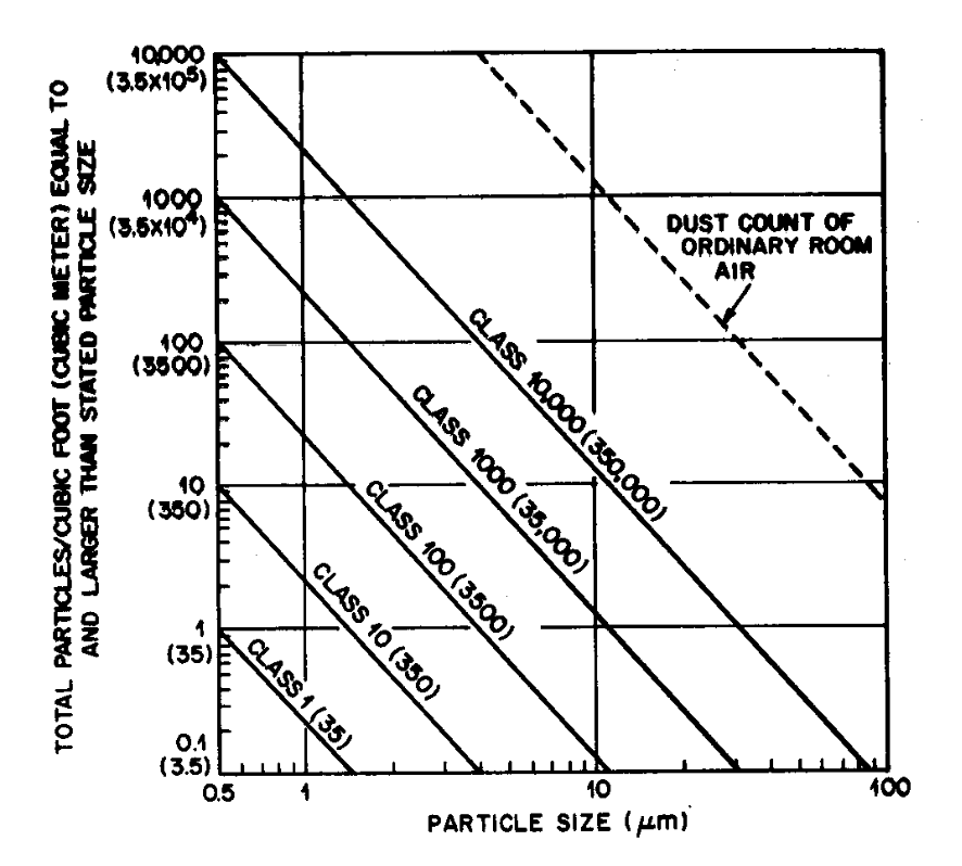
From the graph, Class 1000 has ~1 particle/ft³ (≈35/m³) of size >10µm. Normal room air has ~1000 particles/ft³ (≈35,000/m³) at >10µm. Volume of air passing over the cell in 5 min: area × velocity × time = (1×10⁻⁴ m²) × (50 m/min) × (5 min) = 0.025 m³. Class 1000: 35 × 0.025 ≈ 0.9 particles (≈1 particle). Normal room: 35,000 × 0.025 ≈ 875 particles. This demonstrates why cleanrooms are essential — nearly 1000× fewer contaminants.
Question
- Describe the typical process steps involved in the production of a GaAs-based LED. Name and describe the key apparatus used in the fabrication process.
Answer
Steps: (1) Epitaxial growth of n- and p-type GaAs/AlGaAs layers on a GaAs substrate, (2) Photolithography to define device mesas, (3) Etching to isolate individual devices, (4) Metallisation for ohmic contacts (top and bottom), (5) Dicing and packaging. Key apparatus: MOCVD reactor (epitaxial growth of III-V layers with precise composition control), mask aligner (UV lithography for pattern transfer), wet/dry etcher (mesa formation), metal evaporator/sputterer (contact deposition), wire bonder (connecting die to package leads).
Question
- Why is UV light typically used in optical lithography? Why does electron beam lithography provide a higher spatial resolution? What are the advantages and disadvantages of each approach?
Answer
UV light: shorter wavelength than visible → smaller diffraction-limited features (resolution ∝ λ). DUV at 193nm enables sub-100nm features with immersion/multi-patterning. E-beam: electrons at typical accelerating voltages have de Broglie wavelengths of ~pm, far below UV, enabling sub-10nm resolution. UV advantages: parallel exposure (entire wafer at once), high throughput, low cost per wafer. Disadvantages: diffraction-limited resolution, expensive masks. E-beam advantages: highest resolution, maskless (direct write), flexible for prototyping. Disadvantages: serial process (very slow), low throughput, not viable for mass production.
Question
- What are the differences between a positive and negative resist?
Answer
Positive: exposed regions become soluble in developer (chain scission). Pattern on wafer matches the mask. Better resolution, used for fine features. Negative: exposed regions crosslink and become insoluble. Pattern on wafer is the inverse of the mask. More robust/chemically resistant but prone to swelling, limiting resolution. Generally used for less critical layers.
Question
- Explain the advantage of using a Phase-Shifting Mask compared with a Binary Mask.
Answer
Binary mask: chrome on glass, either blocks or transmits light. At feature edges, diffraction causes intensity spread, limiting resolution. Adjacent bright features can blur together. Phase-shifting mask: alternating transmission regions have a 180° phase shift (achieved by etching the glass to a specific depth). Where light from adjacent openings overlaps, destructive interference creates a sharp dark boundary. This significantly improves edge contrast and resolution, enabling smaller features than the diffraction limit of a binary mask would allow.
Question
- Describe the lift-off process for making metal contacts.
Answer
Steps: (1) Spin coat photoresist on wafer, (2) Expose and develop to create openings where contacts are needed — ideally with an undercut (re-entrant) profile, (3) Deposit metal over entire surface (evaporation preferred for directional deposition), (4) Dissolve resist in solvent — metal on the resist lifts off, metal in the openings remains bonded to the semiconductor. The undercut profile is critical: it creates a shadow during deposition ensuring a clean discontinuity between metal on the substrate and metal on the resist, enabling clean lift-off.
Question
- Describe the key differences between a Schottky and an Ohmic contact.
Answer
Schottky: metal-semiconductor junction with a potential barrier (Schottky barrier). Exhibits rectifying (diode-like) I-V behaviour — current flows easily in one direction. Used in Schottky diodes, gate contacts on FETs.
Ohmic: linear I-V characteristic (V = IR), no barrier to current flow in either direction. Achieved by heavily doping the semiconductor surface so carriers can tunnel through the thin barrier. Used for source/drain contacts, LED contacts — anywhere low-resistance bidirectional contact is needed.
Question
- What is the Damascene process and why is it used?
Answer
A metallisation technique where trenches/vias are first etched into a dielectric layer, then filled with metal (typically copper by electroplating), and excess metal is removed by chemical-mechanical polishing (CMP) to leave metal only in the trenches. Used because copper is difficult to etch by conventional plasma methods (non-volatile etch products). The Damascene process avoids the need to etch copper directly and produces planar surfaces essential for multilayer interconnects in modern ICs.
Question
- Why are test structures added to mask sets? What are the pros and cons? Give one example.
Answer
Purpose: monitor process parameters and quality control without sacrificing device area. Pros: enable in-line measurement of critical parameters (sheet resistance, contact resistance, line width, alignment accuracy), early detection of process drift, improved yield. Cons: consume wafer area (placed in scribe lanes to minimise this), add mask complexity, may not perfectly represent conditions in the active device area. Example: Transmission Line Model (TLM) structure — a series of metal contacts with varying spacing on a doped region. Measuring resistance vs gap length gives both contact resistance (y-intercept) and sheet resistance (gradient).
Question
- Describe three types of hazards in cleanrooms.
Answer
(1) Chemical: toxic, corrosive, and flammable chemicals (HF, H₂SO₄, organic solvents, toxic gases like arsine/phosphine). Require fume hoods, PPE, and gas monitoring. (2) Electrical: high-voltage equipment (plasma etchers, ion implanters, e-beam systems). Risk of electrocution and arc flash. (3) Radiation: UV exposure from lithography tools, laser radiation from alignment and characterisation systems. Require shielding, interlocks, and laser safety protocols.
Question
- Define “Threshold Limit Values (TLV)” and “Immediately Dangerous to Life and Health (IDLH)” in the context of chemical hazards.
Answer
TLV: the maximum airborne concentration of a substance that a worker can be exposed to repeatedly (typically 8-hour TWA) without adverse health effects. Set by occupational health bodies as safe working limits. IDLH: the concentration that poses an immediate threat to life, would cause irreversible health effects, or would impair a worker’s ability to escape. Exposure at IDLH levels requires immediate evacuation and use of self-contained breathing apparatus. IDLH values are always significantly higher than TLV values.