In CMOS, we alternate PMOS and NMOS on a single substrate:
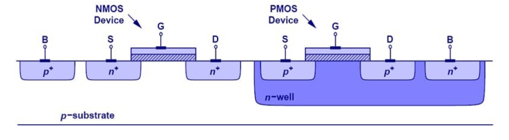 This means we need large, deep n- wells to be created for our PMOS devices with shallow p+ and n+ contacts.
Diffusion is usually done in a furnace (at for Si)
Sources:
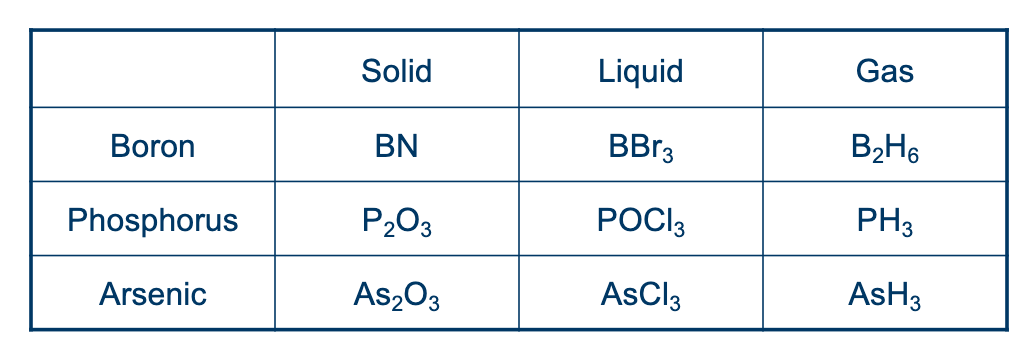
Normally you use an inert carrier gas to carry and then reduce at the surface
Diffusion Mechanism
Generally at higher temperatures, individual lattice atoms can gain enough energy to leave the lattice and become interstital atoms. A impurity atom will then migrate to this vacancy
Where is a constant and is an activation energy, usually 0.5-1.5eV for interstital diffusion, and 2-3eV for vacancy diffusion
Dopant Concentration
Fick’s Law:
We can say that the flux is proportional to the concentration gradient and atoms move away from regions of high concentration to low concentration. Let us consider the diffusion fluxes in and out of a small volume at position x and thickness dx
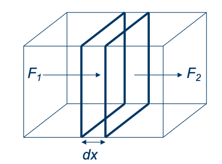
We can then derive that:
This is known as the diffusion equation. It is a second order partial differential equation which requires boundary conditions to be soluble.
We can then say that the Total number of Dopant Atoms per Unit Area of Semiconductor () is:
Where is called the diffusion length
Actually at a high enough dopant concentration we start to distort our lattice:
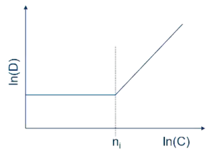
And the previously constant Diffusion coefficient D becomes variable
Dopant Segregation
LOcal Oxidation of Silicon
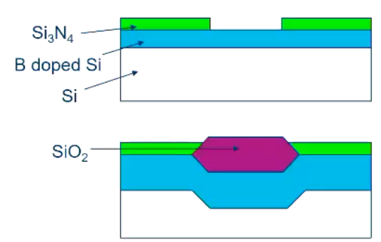
We can use a thin nitride layer to “choose” where we decide to oxidise our silicon.
Segregation Coefficient
When silicon is thermally oxidised, the growing SiO₂ consumes Si at the interface. Dopant impurities near the surface redistribute between the two materials until equilibrium is reached. The direction depends on the segregation coefficient:
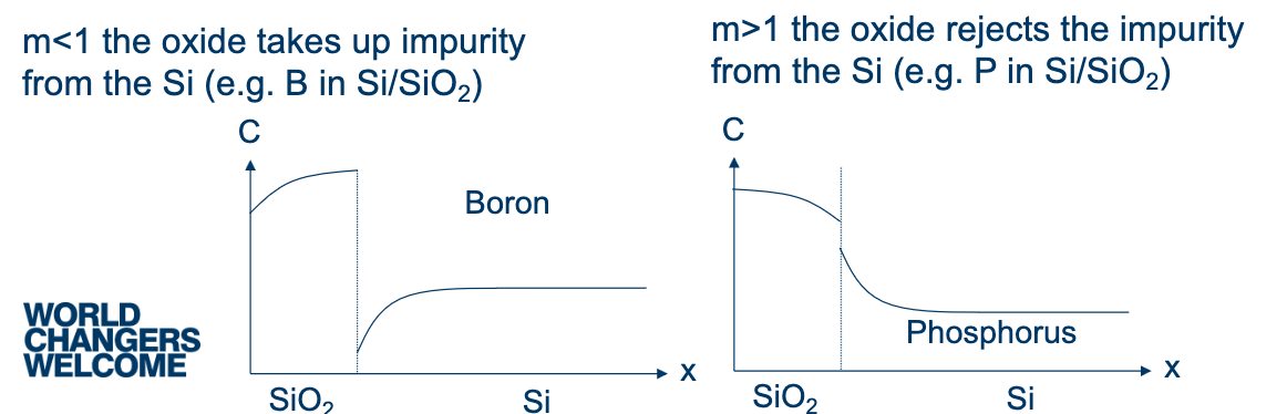
(e.g. Boron): The oxide preferentially takes up the dopant. Boron is drawn out of the Si into the SiO₂, so the Si near the interface becomes depleted. The concentration profile shows a buildup in the oxide and a dip in the Si near the interface. This is a problem for p-type devices — you lose your surface doping during oxidation.
(e.g. Phosphorus): The oxide rejects the dopant. Phosphorus is pushed back into the Si as the oxide front advances, causing a pileup of dopant at the Si side of the interface. The oxide has very low concentration. This actually increases surface doping on the Si side.
This matters practically because thermal oxidation is used extensively in CMOS processing (gate oxides, isolation, etc.), and if your carefully implanted doping profiles get redistributed by the oxidation step, device characteristics shift. You need to account for segregation effects when designing the process flow.