This essentially defines any deterioration in the electrical or optical characteristics of the semiconductor. This is especially problematic in III-V semiconductors that we cant anneal
Elimination of damage is important to advanced devices, particularly FETs and mirrors.
As ions have low energy (50-500eV), they dont amorphise the surface but introduce electrical traps.
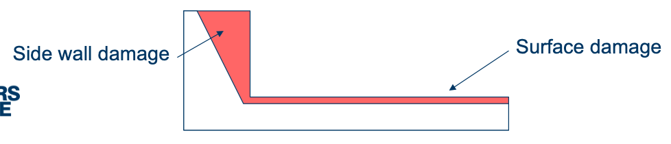
Surface Damage saturates at a certain depth but sidewall increases with dose:
Avoiding Damage
- Use as low energy as possible for ions. This means a low bias voltage for your RIE machine
- Use a high etch rate. You can etch the damaged layer off
- Avoid inert gases like Argon. Argon can stabilise a plasma but a clean chamber is a better way, as argon increases sputtering