Question
- What properties of X-rays make them useful to characterise crystals?
Answer
X-ray wavelengths (~0.1 nm / ) are comparable to interatomic spacings in crystals (~0.1-0.5 nm), enabling diffraction from crystal planes via Bragg’s law: nλ = 2d·sinθ. Their high energy means they penetrate into the bulk (not just surface), and the diffraction pattern reveals lattice constant, crystal structure, orientation, strain, and composition. X-rays interact weakly enough with matter to be non-destructive.
Question
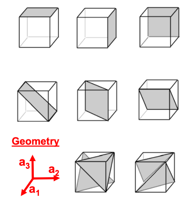
- Calculate the Miller Indices for the planes shown.
Answer
From the diagrams (top row, left to right):
- Plane intercepting a₁=∞ a₂=∞, a₃=1 → (001)
- Plane intercepting a₁=∞, a₂=1, a₃=∞ → (010)
- Plane intercepting a₁=0, a₂=∞, a₃=∞ → (,0,0)
Middle row, left to right:
- Plane intercepting a₁=∞, a₂=1, a₃=1 → (011)
- Plane intercepting a₁=0, a₂=1, a₃=∞ → ()
- Plane intercepting a₁=0, a₂=∞, a₃=1 → ()
Bottom row,
- ()
- ()
Question
- Describe why some of the diffraction orders are absent in body-centred and face-centred crystal structures.
Answer
The additional basis atoms in BCC and FCC unit cells produce extra scattered waves that destructively interfere with those from the corner atoms for certain (hkl) reflections. BCC: the body-centre atom is displaced by (a/2, a/2, a/2) from the corner. Its scattered wave is out of phase when h+k+l is odd, causing destructive interference. Selection rule: reflections present only when h+k+l = even. FCC: face-centre atoms cause destructive interference when h,k,l are mixed odd and even. Selection rule: reflections present only when h,k,l are all odd or all even.
Question
- Describe the basic principle of Photoluminescence (PL). Differences between research and commercial systems?
Answer
A laser with photon energy above the band gap excites electron-hole pairs. Carriers thermalise to band edges and recombine radiatively, emitting photons. The emitted light is collected, dispersed by a spectrometer, and detected.
Research systems: tuneable excitation source, high-resolution monochromator, sensitive cooled detectors (InGaAs, Ge, PMT), cryostat for temperature-dependent measurements (4K-300K), lock-in detection for low signal levels. Can measure fine spectral features, defect peaks, and temperature dependence.
Commercial/production systems: fixed excitation wavelength, room temperature only, lower spectral resolution, faster measurement. Designed for wafer mapping — quickly scanning PL peak wavelength and intensity across the wafer to check uniformity, composition, and material quality.
Question
- Describe the Hall Effect measurement. Sketch a typical setup. What parameters can be extracted?
Answer
Setup: rectangular semiconductor sample with four contacts. Current Ix flows along the length (x-direction). Magnetic field is applied perpendicular to the sample (z-direction). The Lorentz force deflects carriers sideways (y-direction), building up charge on one edge until the transverse electric field balances the magnetic force. The resulting transverse voltage is the Hall voltage .
where d is the sample thickness.
Extractable parameters:
- Hall coefficient: → gives carrier concentration
- Carrier type: sign of indicates n-type (negative ) or p-type (positive )
- Mobility: μ = ||/, where is obtained from a separate resistivity measurement
- Combined with van der Pauw → sheet resistance and Hall mobility simultaneously
Question
- Germanium sample: n-type, Nd = 5×10¹⁵ cm⁻³, d = 5×10⁻³ cm, W = 2×10⁻² cm, L = 0.1 cm, Vx = 100 mV, Ix = 0.25 mA, Bz = 50 mT. Calculate electron mobility.
Answer
First find resistivity from the sample resistance: R = = 0.1/0.25×10⁻³ = 400 Ω R = → = 400 × (2×10⁻²)(5×10⁻³)/(0.1) = 400 × 10⁻³ = 0.4 Ω·cm
In the saturation region, n = = 5×10¹⁵ cm⁻³. = 1/(5×10¹⁵ × 1.6×10⁻¹⁹ × 0.4) = 1/(3.2×10⁻⁴) = 3125 cm²/V·s
μ ≈ 3100 cm²/V·s, which is reasonable for lightly doped Ge at room temperature.
Question
- Sketch how electron mobility of a heavily doped n-type semiconductor varies with temperature. Explain the shape.
Answer
The plot shows μ vs T on a log-log scale with a peak at an intermediate temperature.
Low temperature: mobility increases with T (μ ∝ T^(3/2)). Dominated by ionised impurity scattering — at low T, carriers move slowly and spend more time near ionised dopants, scattering strongly. As T increases, carriers have more thermal energy and are deflected less by the Coulomb potential.
High temperature: mobility decreases with T (μ ∝ T^(-3/2)). Dominated by lattice (phonon) scattering — more phonons are thermally excited at higher T, increasing the scattering rate.
For heavily doped material, the impurity scattering contribution is larger and extends to higher temperatures, shifting the peak to higher T and reducing the overall peak mobility compared to lightly doped material.
Question
- Van der Pauw: three requirements and typical sample geometry.
Answer
Requirements: (1) Sample must be flat and of uniform thickness. (2) Sample must be homogeneous and isotropic. (3) Four ohmic contacts must be placed at the periphery of the sample. Also: no isolated holes in the sample.
Typical geometry: square or cloverleaf shape. The cloverleaf design forces current to flow through narrow arms, reducing errors from finite contact size. Contacts at the four tips of the cloverleaf. Two sets of resistance measurements (R₁₂,₃₄ and R₂₃,₄₁) are taken and combined via the van der Pauw equation: .
Question
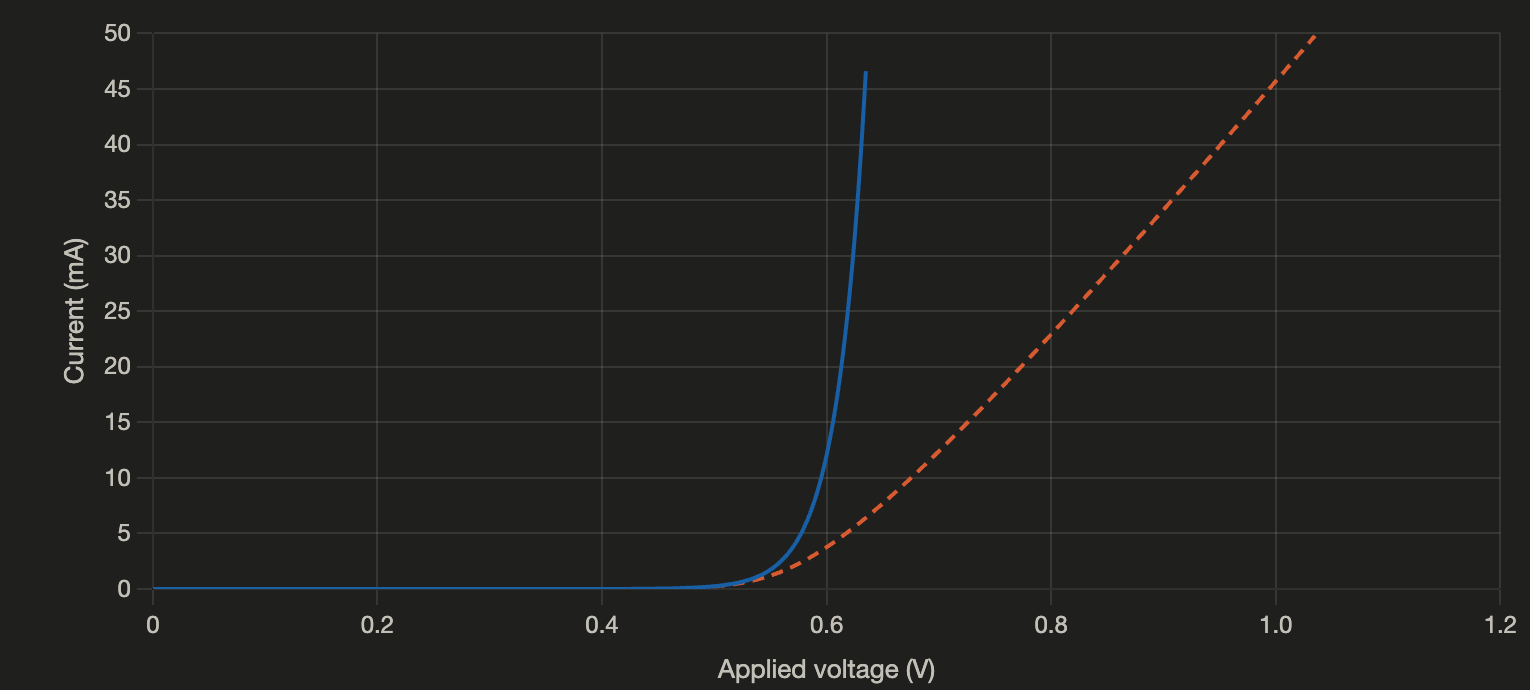
- Sketch forward bias I-V for (a) an ideal diode and (b) a diode with series resistance. Impact on LED/solar cell?
Answer
(a) Ideal: . Exponential rise after turn-on voltage (~Eg/q). Sharp knee. (b) With series resistance Rs: at high currents, V across the junction is reduced by IRs, so the I-V curve bends over and becomes more linear at high current. The exponential shape flattens — effectively V_applied = V_junction + IRs.
Impact on LED: higher operating voltage for a given current → increased electrical power dissipation (I²Rs heating) → reduced wall-plug efficiency, potential thermal degradation. Impact on solar cell: reduces fill factor (the I-V curve becomes less rectangular). Power at the maximum power point decreases. Rs causes voltage drop under load, directly reducing output power and conversion efficiency.
Question
- What physical properties are useful to measure for an LED? Describe the experimental techniques.
Answer
Key properties and measurement techniques:
(1) Emission spectrum (peak wavelength, FWHM): measured using a spectrometer/monochromator with appropriate detector. Gives emission wavelength (colour) and spectral purity.
(2) Light output power vs current (L-I): photodetector or integrating sphere measures total optical output as a function of drive current. Gives external quantum efficiency, wall-plug efficiency, and identifies efficiency droop.
(3) I-V characteristic: source-measure unit sweeps voltage and measures current. Gives turn-on voltage, series resistance, ideality factor, and leakage current.
(4) Angular emission pattern (radiation pattern): goniometer with photodetector measures intensity vs angle. Important for beam shaping and application design.
(5) Temperature dependence: repeat L-I and spectral measurements at different temperatures (thermoelectric stage). Reveals thermal stability and efficiency loss mechanisms.
(6) Reliability/lifetime: operate at elevated current/temperature and monitor output power over time. Gives degradation rate and projected lifetime.