Transfer Length Model (TLM)
Linear Transfer Length Model (LTLM)
Link to original
is the transfer length — the distance over which most of the current transfers from the semiconductor into the contact. It’s derived from the ratio of contact resistivity to sheet resistance.
This is just the rearrangement of the above — once you extract from the x-intercept of the LTLM plot (resistance vs. contact spacing) and know from the slope, you get .
/../../../Year5/MicroAndNanotechnology/Pasted-image-20260422115243.png)
Circular Transfer Length Model (CTLM)
Link to original
No need for mesa etch, easier to manufacture
C-V Profiling
The depletion region of a p-n junction acts as a parallel plate capacitor:
where is the permittivity, is the junction area, and is the depletion width.
When increases by , the charge exposed is , so:
From (1), , so (3).
Substituting (3) into (2) and rearranging gives a separable ODE:
Integrating:
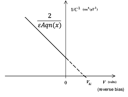
The boundary condition is that when , all the depletion region has collapsed, which occurs at (the built-in voltage). This gives the key result:
How you use it: plot vs reverse bias . For uniform doping it’s a straight line where:
- The slope gives the doping concentration
- The x-intercept gives the built-in voltage
For non-uniform doping, the slope varies with and you extract the local doping profile at each bias point from the local gradient.