Question
- Explain why silicon has dominated electronics. Why has silicon not similarly dominated photonics? What semiconductors are mainly used to make LEDs and lasers and why? Give some examples.
Answer
Silicon dominates electronics due to: suitable bandgap (~1.1eV), stable native oxide (SiO₂) for gate insulators, abundance (cheap), and mature processing technology. It hasn’t dominated photonics because its indirect band gap makes radiative recombination inefficient. LEDs and lasers use direct band gap III-V semiconductors: GaAs (~870nm IR), InGaAsP (1.3-1.55µm telecom), GaN (blue/UV LEDs), InGaAlP (red/orange LEDs).
Question
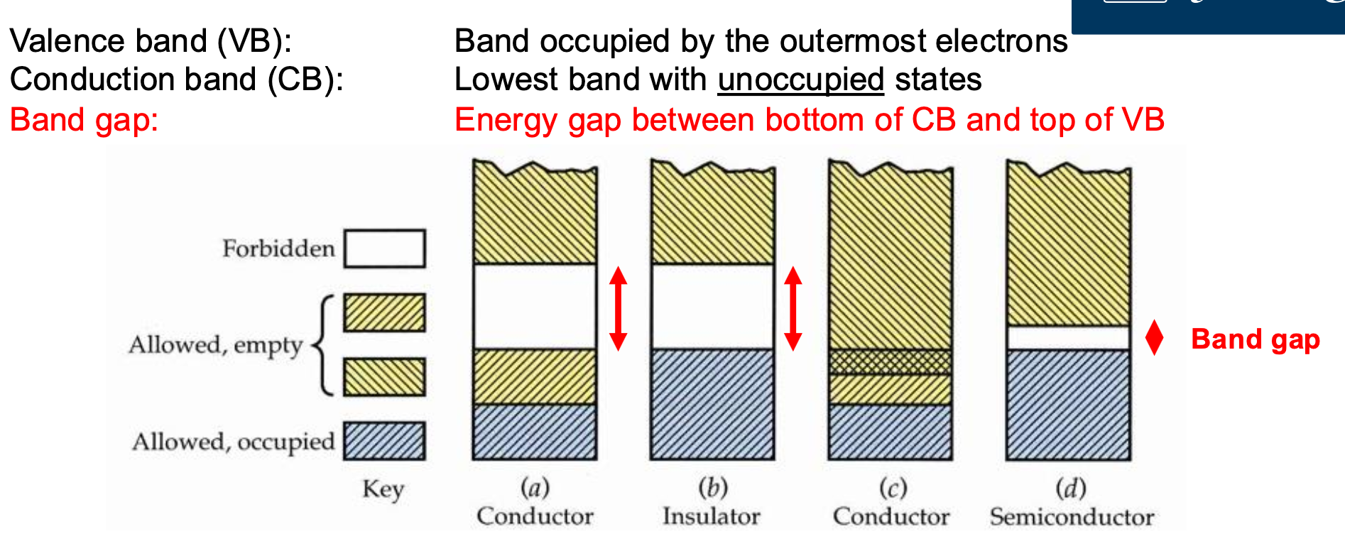
- State the key differences between semiconductors, metals and insulators.
Answer
Metals: no band gap, partially filled conduction band, high conductivity, decreases with temperature. Insulators: large band gap (>~4eV), negligible carriers at room temperature. Semiconductors: moderate band gap (~0.5-3eV), conductivity tuneable via doping and temperature, conductivity increases with temperature.
Question
- Explain how (a) temperature and (b) illumination with light alter the properties of semiconductors. In each case, give an example of how these effects can be exploited in devices.
Answer
(a) Temperature: thermal energy excites electrons across the band gap, increasing carrier concentration and conductivity. Exploited in thermistors (temperature sensors) — resistance changes measurably with temperature. (b) Illumination: photons with E ≥ Eg generate electron-hole pairs, increasing conductivity (photoconductivity). Exploited in solar cells (pn junction separates photogenerated carriers) and photodetectors.
Question
- What is Moore’s Law? Describe any limitations in how it can continue.
Answer
Empirical observation by Gordon Moore (1965) that transistor count on a chip doubles approximately every two years. Limitations: atomic-scale limits (can’t make features smaller than atoms), quantum tunnelling through thin barriers causing leakage, power density and heat dissipation, lithography resolution limits, increasing fabrication costs per node.
Question
- Describe the key process steps used to turn sand into silicon wafers.
Answer
This is done in an arc furnace () forming MGS (99%) and then we grind, and heat to and then with this we decompose onto hot silicon rods at to form to form 99.999999% pure Si. We then use CZ Growth to form long boules which get sliced in wafer
Question
- What is meant by the “band gap” of a semiconductor. Describe why it is important in terms of semiconductor device properties. Give an example.
Answer
The energy difference between the valence band maximum and conduction band minimum. It determines: minimum photon energy for absorption/emission, intrinsic carrier concentration, operating temperature range, and emission wavelength for LEDs/lasers (λ = hc/Eg). Example: GaAs Eg = 1.42eV → emits at ~870nm (near-IR), used in IR LEDs and telecom lasers.
Question
- Which of the following semiconductors are transparent (or partially transparent) to visible light (400-700nm): Si, GaN, GaP and GaAs? State why.
Answer
Visible photon energies: ~1.8-3.1eV. A semiconductor is transparent when Eg > photon energy.
- Si (1.1eV): absorbs all visible → opaque
- GaAs (1.4eV): absorbs all visible → opaque
- GaP (2.26eV): transparent to red/orange, absorbs blue/green → partially transparent
- GaN (3.4eV): Eg above visible range → transparent
Question
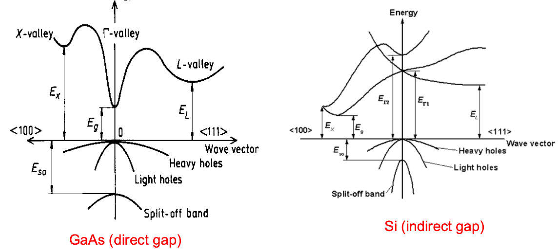
- What is the difference between a direct and indirect band gap semiconductor. Show why direct band gap semiconductors are more useful for light emitting devices.
Answer
Direct: conduction band minimum and valence band maximum at the same k-vector (momentum). Electron-hole recombination emits a photon directly (momentum conserved). Indirect: band extrema at different k-vectors, so recombination requires a phonon to conserve momentum. This is a three-body process with much lower probability, making radiative recombination inefficient. Direct band gap materials (GaAs, GaN, InP) are therefore far more efficient light emitters.
Question
- Describe what is meant by a “hole” and why it can be treated as a charge carrier. Describe how both holes and electrons can carry a current.
Answer
A hole is a vacant electron state in the valence band. When a neighbouring valence electron fills the vacancy, the hole effectively moves in the opposite direction. It behaves as a positive charge carrier with its own effective mass. Under an electric field, electrons drift opposite to the field and holes drift with the field — both contribute to current:
Question
- What is meant by “doping” a semiconductor? Describe how donors and acceptors work. Give examples for silicon.
Answer
Doping: intentionally introducing impurity atoms to control carrier concentration. (a) Donors (n-type): group V atoms (e.g. phosphorus, arsenic) replace Si in the lattice. They have 5 valence electrons — 4 form bonds, the 5th is loosely bound and easily ionised into the conduction band, donating a free electron. (b) Acceptors (p-type): group III atoms (e.g. boron, gallium) have only 3 valence electrons — they accept an electron from the valence band to complete bonding, creating a hole.
Question
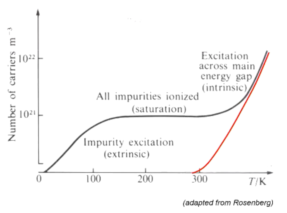
- Describe the difference between an intrinsic and extrinsic semiconductor. Sketch free carrier concentration versus temperature.
Answer
Intrinsic: pure, undoped. n = p = nᵢ, determined solely by thermal generation. Extrinsic: doped, one carrier type dominates.
Question
- Derive the built-in potential of a pn junction.
Answer
When p-type and n-type materials are joined, carrier diffusion creates a depletion region with an electric field opposing further diffusion. At equilibrium, the Fermi level is constant across the junction. In n-type: In p-type: Built-in potential: (before contact) = So
Question
- Show how a pn junction forms a diode. Draw the I-V characteristic. What is reverse breakdown?
Answer
The pn junction acts as a diode: forward bias reduces the barrier → exponential current increase . Reverse bias widens the depletion region → only small leakage current (I₀) flows. I-V characteristic: exponential rise in forward bias, near-zero current in reverse until breakdown.
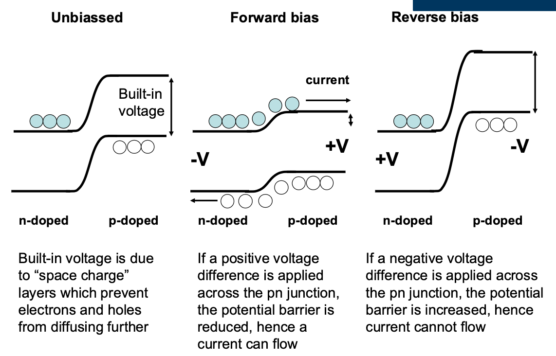
Reverse breakdown: at sufficiently high reverse voltage, avalanche multiplication (impact ionisation) or Zener tunnelling causes a sharp increase in reverse current. Application: Zener diodes used as voltage references/regulators.
Question
- Describe how pn junction diodes can be used to form half-wave and full wave rectifier circuits.
Answer
Half-wave: single diode in series with load. Conducts on positive half-cycles, blocks negative — output is pulsating DC with half the input frequency content missing.
Full-wave: four diodes in a bridge configuration. On each half-cycle, two diodes conduct and two block, routing current through the load in the same direction regardless of input polarity. Output has double the ripple frequency, easier to smooth with a capacitor.
Question
- Describe how pn junctions can be used to form bipolar junction transistors. What can these transistors be used for?
Answer
BJT: two back-to-back pn junctions forming NPN or PNP structure (emitter, base, collector). The thin, lightly doped base allows minority carriers injected from the forward-biased emitter-base junction to diffuse across and be swept into the collector by the reverse-biased collector-base junction. Small base current controls large collector current (current gain β = Iᶜ/Iᴮ). Applications: amplification (analogue circuits) and switching (digital logic, power electronics).
Question
- Describe the operating principle of a Field Effect Transistor (FET).
Answer
A voltage applied to the gate electrode modulates the conductivity of a channel between source and drain. In a MOSFET: gate voltage creates an electric field through the oxide insulator that attracts/repels carriers in the semiconductor, forming or depleting a conductive channel. Current flows between source and drain proportional to the channel conductance. Key advantage over BJT: voltage-controlled (high input impedance), lower power, dominant in CMOS logic.
Question
- Describe the three optical processes that occur in semiconductors. In each case provide an example of a device that exploits the process.
Answer
(1) Absorption: photon with E ≥ Eg excites an electron from valence to conduction band, creating an electron-hole pair. Device: solar cell, photodetector. (2) Spontaneous emission: electron-hole recombination emits a photon randomly in direction and phase. Device: LED. (3) Stimulated emission: incoming photon triggers recombination, producing a second photon identical in wavelength, phase, and direction. Device: semiconductor laser (requires population inversion and optical feedback).