Scanning Probe Microscopy Tutorial Questions
Question
- What is the primary function of Scanning Probe Microscopy (SPM)? A) To examine the chemical composition of materials B) To observe live cells in their natural environment C) To measure the electrical conductivity of materials D) To observe and measure the surface structure of materials at the nanoscale E) To magnify images using lenses like in optical microscopy
Answer
D
Question
- Which of the following is NOT a type of Scanning Probe Microscopy? A) AFM B) STM C) SEM D) MFM E) NSOM
Answer
C SEM uses a focused electron beam and detectors — it’s electron microscopy, not probe microscopy. SPM techniques (AFM, STM, MFM, NSOM) all use a physical probe scanned across the surface.
Question
- In AFM, what is the primary purpose of the cantilever? A) To emit electrons onto the sample surface B) To detect the reflected light from the sample C) To hold the probe that interacts with the sample, bending in response to forces D) To illuminate the sample with UV light E) To collect secondary electrons
Answer
C The cantilever deflects in response to tip-sample interaction forces. A laser reflected off the cantilever back onto a photodetector measures this deflection with sub-angstrom sensitivity.
Question
- Which factor primarily limits the resolution of an STM? A) Light source intensity B) Wavelength of electrons C) Sharpness of the probe tip D) Distance between probe and sample E) Speed of scanning
Answer
C Tunnelling current is dominated by the atom at the very apex of the tip. A sharper tip (ideally terminating in a single atom) gives better lateral resolution. Tip quality is the main practical limitation.
Question
- What unique capability does STM offer compared to other SPM types? A) Measure force between tip and sample B) Manipulation of individual atoms and molecules on a surface C) Image biological samples in liquid D) Uses a laser to detect tip position E) Image without contacting the surface
Answer
B STM can push, pull, and position individual atoms on surfaces by adjusting tip-sample voltage and distance. Famously demonstrated by IBM spelling “IBM” with xenon atoms on nickel in 1990.
Question
- PZT has ~0.3 nm/V expansion. How many volts for 1 µm deflection?
Answer
V = 1000 nm / 0.3 nm/V ≈ 3333 V ≈ 3.3 kV
Question
- Identify at least four important artefacts in AFM images.
Answer
(1) Tip convolution: finite tip radius broadens features, making objects appear wider than they are. (2) Tip asymmetry: asymmetric tip shape causes directional distortion of features. (3) Scanner hysteresis/creep: piezoelectric nonlinearity causes spatial distortion, especially at scan edges. (4) Thermal drift: temperature changes cause slow spatial drift during imaging. Also: feedback artefacts (overshoot at step edges), scanner bow (apparent curvature on flat surfaces), and contamination on the tip.
Question
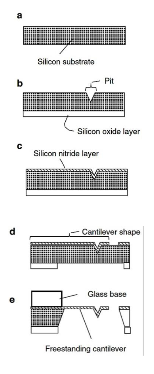
- AFM Si cantilever: l = 100 µm, w = 10 µm, t = 1 µm, ρ = 2330 kg/m³, E = 179 GPa. Calculate a) The mass of the cantilever. b) The spring constant for normal bending using the formula: kN = (E w t3)/(4 l3). c) The resonance frequency (in Hz) of the cantilever associated with normal bending. d) The five steps sketched below show snapshots in the process of manufacturing a freestanding AFM Silicon Nitride cantilever. Briefly describe the process necessary to go from a to b, b to c, c to d, and d to e
Answer
a) Mass: m = ρ × V = 2330 × (100×10⁻⁶)(10×10⁻⁶)(1×10⁻⁶) = 2330 × 10⁻¹⁵ = 2.33×10⁻¹² kg = 2.33 pg
b) kN = Ewt³/(4l³) = 179×10⁹ × 10×10⁻⁶ × (1×10⁻⁶)³ / (4 × (100×10⁻⁶)³) = 179×10⁹ × 10⁻⁵ × 10⁻¹⁸ / (4 × 10⁻¹²) = 1.79×10⁻¹² / 4×10⁻¹² = 0.4475 N/m ≈ 0.45 N/m
c) f₀ = (1/2π)√(k/m*) where m* ≈ 0.24m for a cantilever beam m* = 0.24 × 2.33×10⁻¹² = 5.59×10⁻¹³ kg f₀ = (1/2π)√(0.4475/5.59×10⁻¹³) = (1/2π)√(8.00×10¹¹) = (1/2π)(8.94×10⁵) ≈ 142 kHz
d) a→b: Anisotropic wet etch (e.g. KOH) of silicon to create a pit/pyramid (defines the tip shape). b→c: Deposit silicon nitride layer (e.g. LPCVD) over the entire surface including into the pit. c→d: Pattern the silicon nitride using lithography and etching to define the cantilever shape. d→e: Etch away the silicon substrate from behind (selective etch stops at Si₃N₄), bond to a glass base, leaving a freestanding cantilever with an integrated tip.