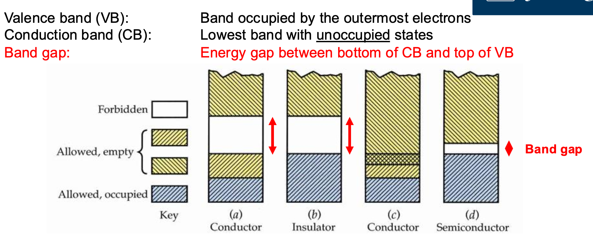
Semiconductors are useful because unlike metals which just conduct, or insulators that dont conduct at all, we can control whether semiconductors conduct under given circumstances.
Uses of Semiconductors
Many different things can affect the conductivity of a semiconductor, such as:
| Type of Device | |
|---|---|
| Doping | Diodes |
| Temperature | Thermometers |
| Magnetic Field | Hall Effect |
| Light | Photodiode |
| Voltage | Field Effect Transistor (FET) |
| Current | Bipolar Junction Transistor (BJT) |
| Basic properties of conduction and light absorption are affected by “band structure”, making these Quantum Solids |
Types of Semiconductor
- Covalently-bonded
- Inorganic or organic materials
- Crystalline or amorphous
- Tetrahedrally-coordinated (sp3), not graphitic (sp2)
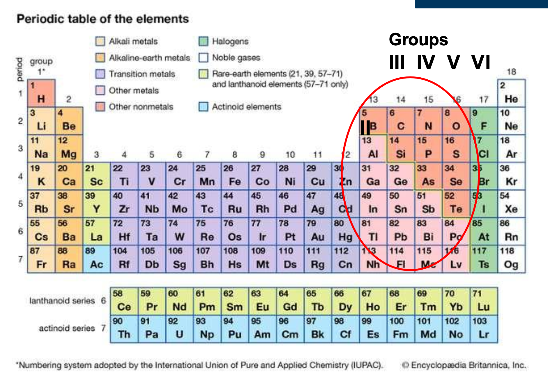
- Elemental, diamond lattice structure, group IV elements or
- Compound, zincblende structure, group III-V (or II-VI)
- Direct-gap or indirect-gap
- Lattice-matched, coherently-strained, or lattice-mismatched
Three main categories:
- Elemental (e.g. Si)
- Compounds (e.g. GaAs)
- Alloys (e.g. AlGaAs)
- Heterostructures (e.g. AlAs/GaAs)
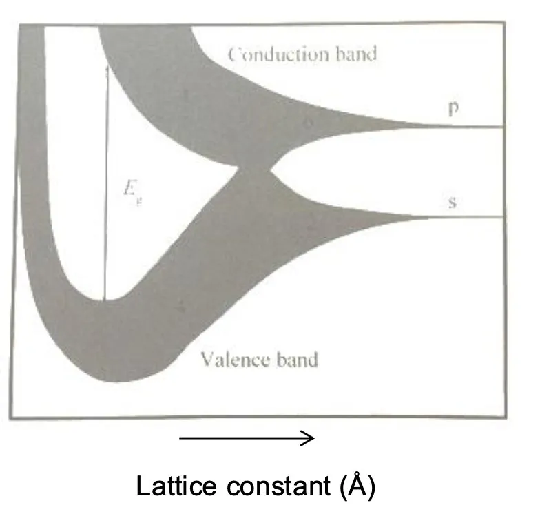 Start with atoms far apart — each has its own energy levels (s and p), completely independent.
Bring them closer — the levels start to smear out into wider bands because neighbouring atoms influence each other. Think of it like tuning forks: one on its own vibrates at a fixed frequency, but put many close together and they couple, creating a range of frequencies instead of one.
Bring them even closer — the s and p bands smear so much they overlap. No gap, so electrons can move freely. This is a conductor.
Closer still — the atoms are now so close that the orbitals don’t just overlap, they fundamentally rearrange into new shared states across the whole crystal. This rearrangement splits the one big merged band back into two separate bands with a gap between them. The bottom band is full of electrons (valence band), the top one is empty (conduction band), and the gap between them is E_g.
So it’s not that the original s and p come back — what comes out of the split are two entirely new bands. The gap exists because of how strongly the atoms are bonded at that spacing.
Where your material’s actual atomic spacing sits on that curve determines whether it’s a metal (in the overlapping region) or a semiconductor (in the re-split region).
Intrinsic vs Extrinsic
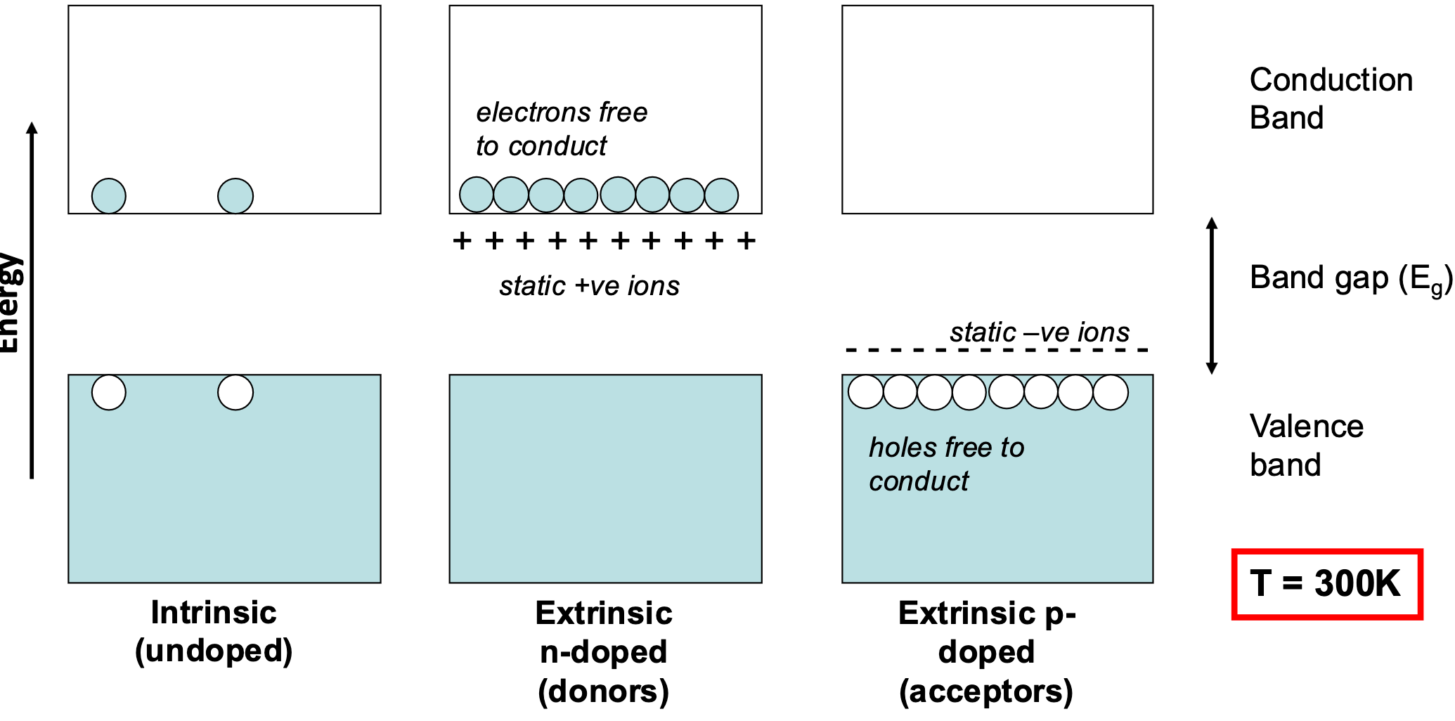
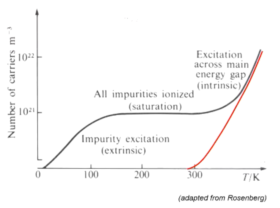
What we find is that in an intrinsic semiconductor we need a lot of thermal energy to get charge jumping across the gap, however in extrinsic, since we have either holes in the valence, or electrons in the conductance, these can move with very little energy. At a certain energy those, these charge carriers become satruated before we get back to the jumping across the band gap again:
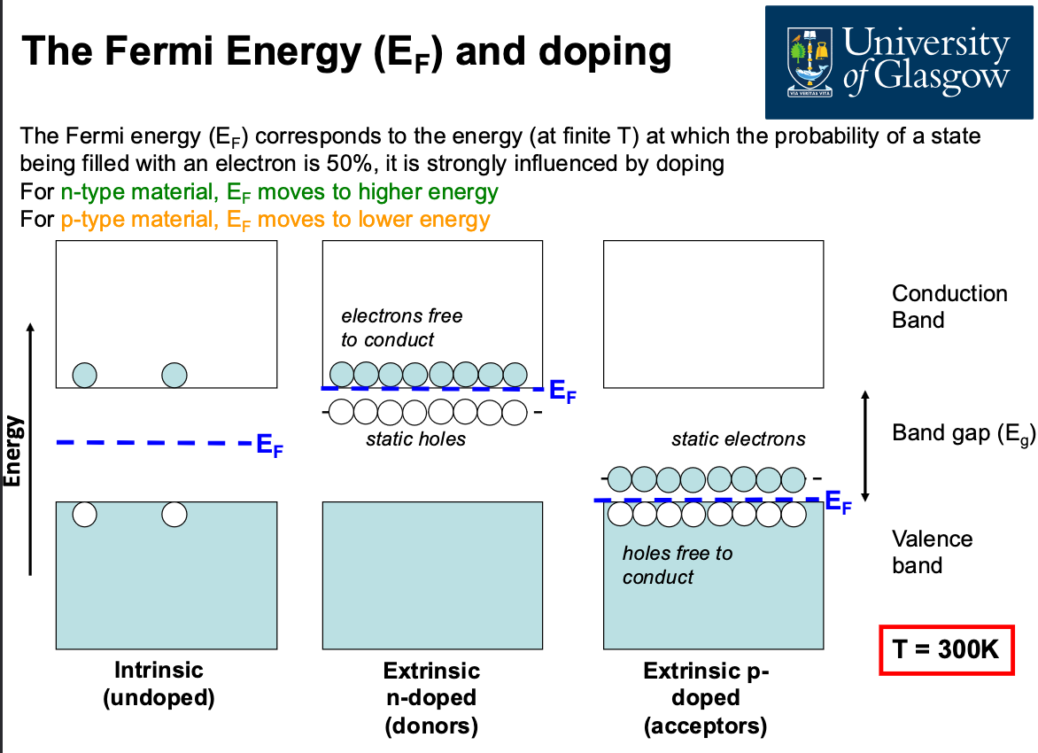
This also relates to Fermi Energy:
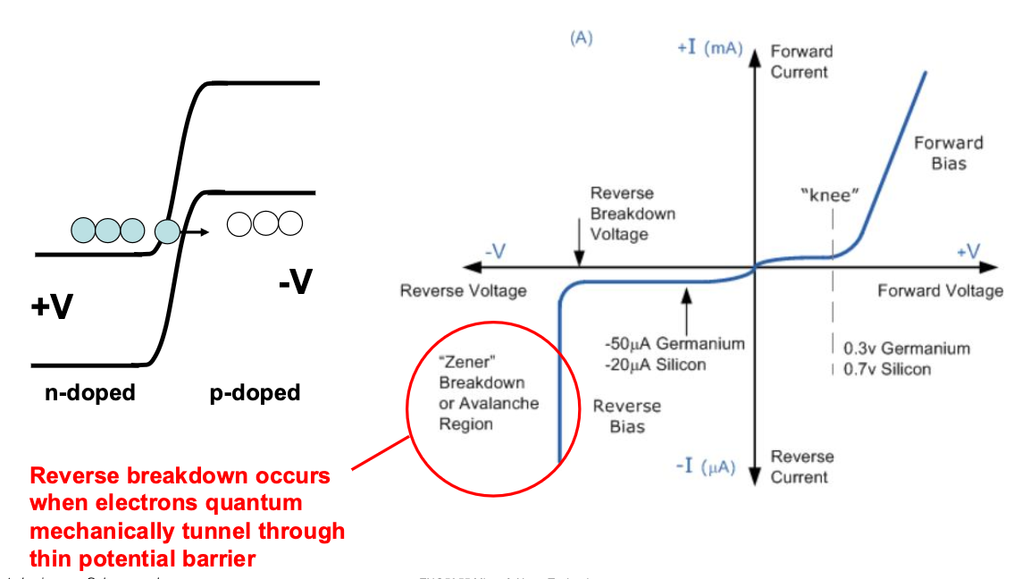
P-N Junctions
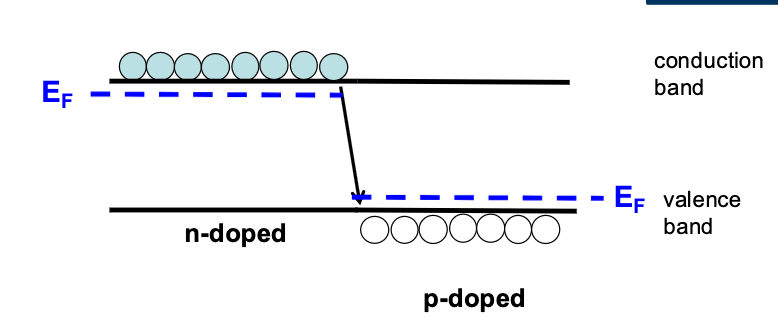
When we put these two regions together, they will naturally want to diffuse, and have holes and electrons recombine. bringing the left sides Fermi energy down and the right side up, this will continue until the Fermi Energies equalise, but the actual gap must remain the same, pushing up what we call a built-in voltage:
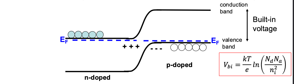 This stops further diffusion at steady state, unless a voltage is applied.
This is where bias becomes important:
This stops further diffusion at steady state, unless a voltage is applied.
This is where bias becomes important:
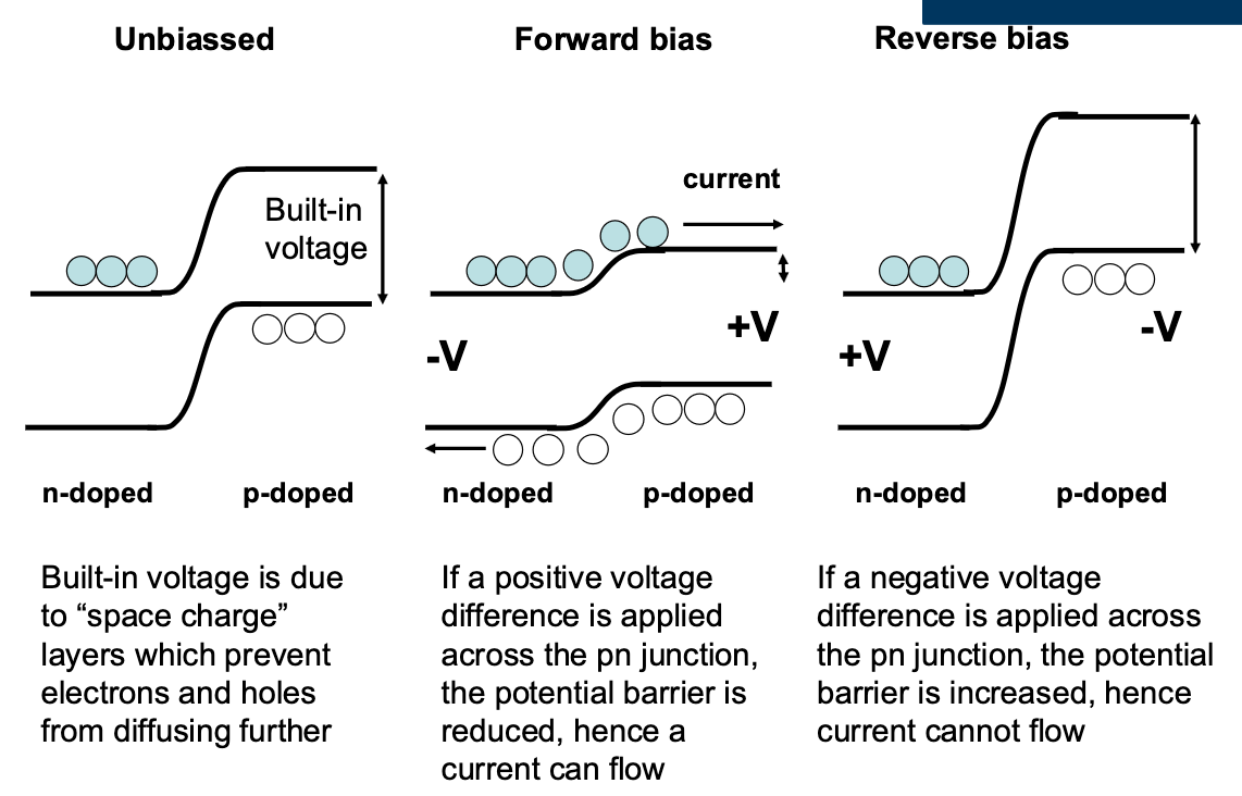
This reverse bias eventually breaks down, having a rectifying ability: