The oxide thickness is an important parameter of the oxidation process, and thus many ways have been developed to measure it.
Physical Determination
It requires the production of a step in the oxide. Typically, this is done with a mask followed by an etch. If a mask is applied to the wafer, the wafer immersed in , and then the mask is removed, then a step nearly equal to the.oxide thickness will be left.
Since part of the oxide must be etched to determine the thickness, this test is destructive and generally requires the use of a dedicated test wafer.
You can measure this with a Scanning Tunnelling Microscope if it is larger than 20nm, or a Tunnelling Electron Microscope otherwise Another approach would be to use a Scanning Profilometer
Electrical Techniques
These are typically the most useful way to check
Capacitance - Voltage Measurement
In the C-V measurements, a dc bias V is applied to the gate, and a small ac signal is applied to obtain the capacitance at the bias applied. The capacitance of the ideal MOS structure is the series combination of the oxide capacitance and the semiconductor capacitance .
When an ideal MOS capacitor is biased with positive or negative voltages, three cases can exist at the semiconductor surface.
In a p-type:
Accumulation:
When a negative voltage is applied to the metal plate, excess positive carriers (holes) will be induced at the interface. In this case, the bands near
the semiconductor surface are bent upward, as shown in Fig. 3a. The corresponding charge distribution is shown on the right side of Fig. 3a, where is the positive charge per unit area in the semiconductor and is the negative charge per unit area in the metal.
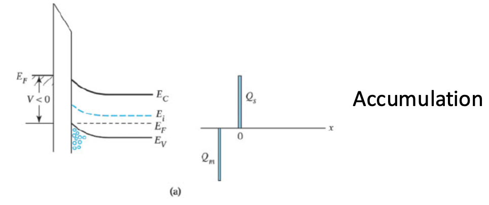
In accumulation
- is the gate area.
- is the permittivity of free space.
- is the relative permittivity (dielectric constant) of the oxide — dimensionless. For SiO₂,
- is the oxide thickness.
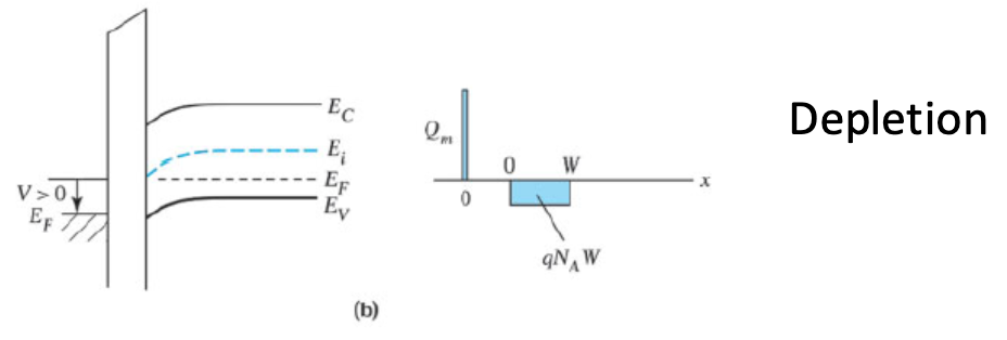
Depletion:
For V > 0 the energy bands near the semiconductor surface are bent downward and the majority carriers (holes) are depleted (Fig. 3b). The space charge per unit area, , in the semiconductor is equal to - , where is the width of the surface depletion region.
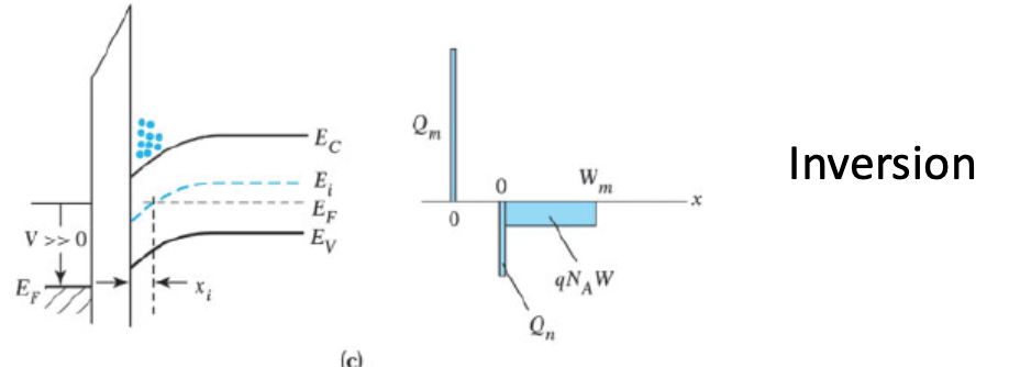
Inversion:
For , the energy bands bend downward even more so that the intrinsic level at the surface crosses over the Fermi level, as shown in Fig 3c. As a result, the positive gate voltage starts to induce excess negative carriers (electrons) at the
interface.
Optical Techniques
Ellipsometry
In this technique, a polarized coherent beam of light is reflected off the oxide surface at some angle. Helium–Neon lasers are commonly used as a source. The reflected light intensity is measured as a function of the polarization angle. By comparing the incident and reflected intensity and the change in the polarization angle, the film thickness and the index of refraction can be found.
To do this definitively requires measurement at more than one incidence angle or for more than one wavelength, since there is more than one thickness that will produce the same change in the light at any given angle or wavelength. Variable angle spectroscopic ellipsometers systematically vary both angle and wavelength and fit the data to a model to extract thickness and index.
Ellipsometry has the advantage of being nondestructive, although it often requires that the oxide be grown on bare silicon. Since the ellipsometer’s beam is quite large, it is also normally done on unpatterned wafers. It is also common to measure many points across the wafer and map the film thickness.
Interference
This technique uses light at a nearly normal incidence to the film. The reflected light intensity is measured as a function of the wavelength. When the wavelength of the light is such that the incoming and outgoing waves constructively interfere, an optical maximum will result. If the waves interfere destructively, a minimum will be seen. By measuring the difference in wavelength Δλ between maxima or minima, the thickness can be determined as
where is the real part of the index of refraction of the oxide; is assumed to be wavelength independent in this model. The technique can measure the thickness of transparent films down to several hundred angstroms. The upper limit for thickness measurement is determined by optical losses in the film and by the ability to resolve high order peaks.
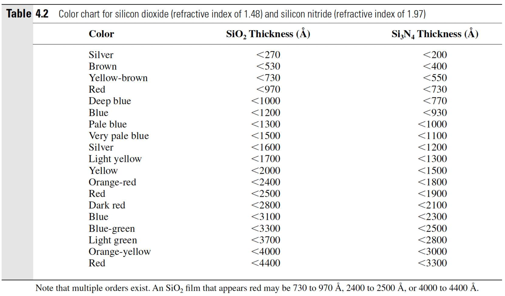
Colour
Oxide is actually colourless but due to the interference of light reflecting off the silicon and the oxide surface we get colours, as the thickness changes, so does the colour.