For a successful scanning microscope we need:
- A rigid construction, an effective vibrational isolation, and a submicron control of the movements to allow reproducible positioning on the atomic scale.
- A scanner and a probe-sample distance control that allows us to scan the probe over the surface and associate interaction with position.
- A probe that sense a short-range interaction, yielding the desired resolution.
A sharp conductive tip is brought extremely close to a conductive sample surface (within ~1 nm). A bias voltage is applied between tip and sample, and electrons quantum mechanically tunnel across the vacuum gap, producing a measurable tunnelling current.
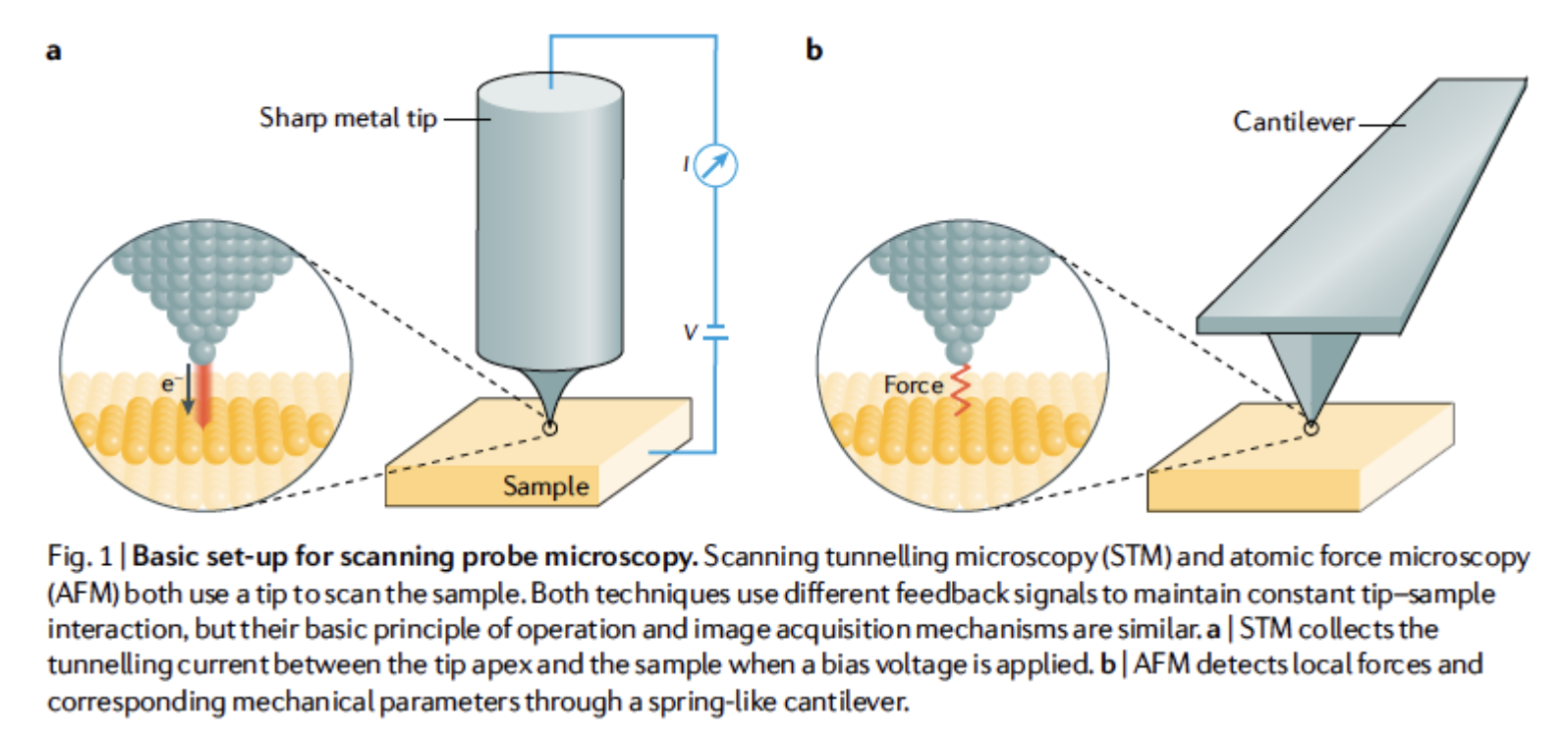
The tunnelling current is exponentially sensitive to the tip-sample distance — even sub-angstrom changes produce significant current variation. This is what gives STM its atomic-scale resolution.
Two operating modes:
- Constant current — a feedback loop adjusts the tip height to maintain a fixed tunnelling current as it scans. The height adjustments map the surface topology.
- Constant height — tip stays at a fixed height and the current variation is recorded directly. Faster, but only works on very flat surfaces.
Key limitations: both the tip and sample must be conductive, and it’s strictly a surface technique. It images the local density of states at the surface, so what you see is electronic structure rather than purely geometric atomic positions — though for most purposes they correspond closely.
The probability that a particle tunnels through a barrier can be expressed as a transmission coefficient () and a reflection coefficient (), where .
If is small:
where:
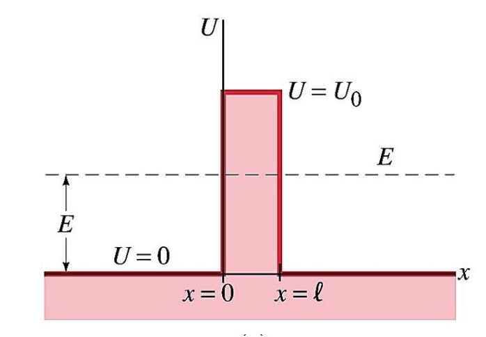
A 10x increase in distance corresponds to a drop in current